Производительность схемы
Еще одно важное правило, о котором следует помнить, - избегать областей, где цифровые схемы пересекают аналоговую проводку и наоборот при подключении в конструкции со смешанным сигналом.


Еще одно важное правило, о котором следует помнить, - избегать областей, где цифровые схемы пересекают аналоговую проводку и наоборот при подключении в конструкции со смешанным сигналом.
Note that this is easier on thinner mediums, where the correspondence between characteristic trace widths and odd-mode trace widths will not be nearly the same.
Несмотря на то, что отрасль быстро развивается от бумажного подхода к проектированию, который в большей степени опирается на автоматизированные инструменты, все еще есть много нюансов, которые следует учитывать при проектировании жестких гибких печатных п
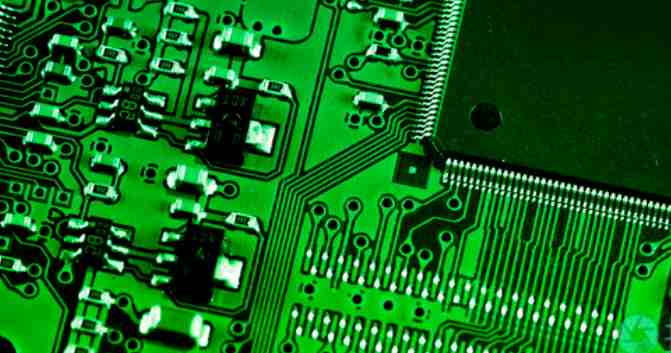
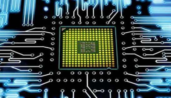
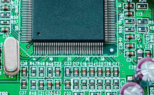
Печатная плата делает схему миниатюрной и интуитивно понятной, что играет важную роль в массовом производстве фиксированной схемы и оптимизации компоновки электроприборов.
During heat treatment, the material's mechanical strength, dimensional stability, adhesion, water absorption, thermal cracking, expansion performance and other aspects are different, high density products are obviously better than ordinary PCB substrate.
The pressing process of printed circuit board is the main process of generating thermal stress. Similar to the pressing process of copper clad plate, it will also produce local stress caused by inconsistency in the curing process. The printed circuit boar
With moisture-proof, anti-corrosion, shock-proof, protection function. Now, you know why to apply three anti-rubber on the circuit board, have the need of small partners do not quickly act.
the color of the circuit board has attracted the attention of the industry, mainly because the color design of many high-end circuit boards are made of green, so people slowly believe that the color of the circuit board is green must be high-end.
It is the latest development in PCB testing technology. It uses a laser beam to scan the printed board, collect all the measurements, and compare the actual measurements with preset qualifying limits.
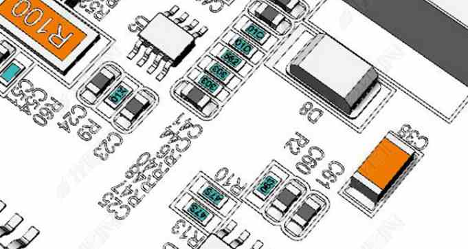
Some people have more information about their designed PCB board, so they like to test all the components at once. In fact, it is better to do it bit by bit.

There are many forms of pcb files. In order to meet different market needs, pcb board manufacturers can open these different forms of files. Then, what materials need to be prepared before pcb board proofing? Follow along to find out!
The shape is not deformed, so as to avoid the deformation of the shell and dislocation of the screw hole after installation. Now are mechanized installation, circuit board hole location and line and design deformation error should be within the allowable


