
Контрактное производство электроники под ключ в Китае
Шэньчжэнь, район Баоань, улица Фуюн, улица Фуцяо, район 3, промышленный парк Лонгхуй 6

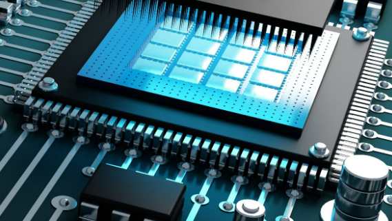
"Cleaning" is often overlooked in the manufacturing process of circuit board (PCB) PCBA as not a critical step. However, with the long-term use of the product in the client, problems caused by ineffective cleaning in the early stage lead to many failures, and repair or recall of the product leads to a sharp increase in operating costs. The following is a brief description of the circuit board (circuit board) PCBA cleaning role.
PCBA (printed circuit components) production process through a number of process stages, each stage is affected by different degrees of pollution, so the PCB (printed circuit board) PCBA surface residual various sediments or impurities, these pollutants will reduce product performance, and even cause product failure. For example, in the process of welding electronic components using solder paste, flux and other auxiliary welding, welding residue, the residue contains organic acids and ions, among which organic acids will corrode the circuit board (circuit board) PCBA, and the presence of electric ions may lead to short circuit, resulting in product failure.
There are many kinds of pollutants on PCBA, which can be summarized into two categories: ionic and non-ionic. Ionic pollutants come into contact with moisture in the environment, and when energized, electrochemical migration occurs, forming dendritic structures, resulting in a low resistance pathway and damaging the PCBA function of the circuit board (circuit board). Non-ionic pollutants can penetrate the insulation layer of PCB and grow dendrites under the surface of PCB board. In addition to ionic and non-ionic pollutants, there are granular pollutants, such as solder ball, solder tank floating point, dust, dust and so on, these pollutants will lead to solder joint quality reduction, welding joint tip, porosity, short circuit and so on a variety of adverse phenomena.

Of all these pollutants, which ones are getting the most attention? Flux or solder paste is widely used in reflow welding and wave soldering process, which mainly consists of solvent, wetting agent, resin, corrosion inhibitor and activator and other components. There must be thermal modified products after welding, and these substances dominate in all pollutants. From the point of view of product failure, post-welding residue is the most important factor affecting product quality. Ionic residue is easy to cause electromigration to reduce insulation resistance, rosin resin residue is easy to adsorb dust or impurities lead to contact resistance increase, serious lead to open circuit failure, so after welding must be strictly cleaned, in order to ensure the quality of circuit board (circuit board) PCBA.
In summary, circuit board (circuit board) PCBA cleaning is very important, "cleaning" is directly related to the circuit board (circuit board) PCBA quality important process, indispensable.
It's so hot, how to cool PCB
Today, many places in Guangdong have issued a high temperature yellow warning signal, the noon Guangdong land, a red fire looks like a trance. In the coming days, people in Guangdong will continue to receive the "love" of rain and sun, according to the observatory, in a "steaming and baking" mode.
Since the weather is so hot, today we will talk about the cooling design of PCB.
For electronic equipment, a certain amount of heat will be generated during work, so that the internal temperature of the equipment will rise rapidly. If the heat is not dissipated in time, the equipment will continue to heat up, and the devices will fail due to overheating, and the reliable performance of electronic equipment will decline. Therefore, it is very important to have a good heat dissipation treatment on the circuit board.
PCB design is the downstream process followed by the principle of design, the quality of the design directly affects the product performance and market cycle. As we know, the devices on PCB board have their own operating environment temperature range, if beyond this range, the working efficiency of the devices will be greatly reduced or failure, resulting in damage to the devices. Therefore, heat dissipation is a key issue to be considered in PCB design.
So, as a PCB design engineer, how to carry out heat dissipation treatment?
PCB heat dissipation and plate selection, selection of components, components layout and other aspects are related. Among them, layout has a decisive role in PCB heat dissipation design, is the key link of PCB heat dissipation design. When making layout, engineers need to consider the following aspects:
(1) The components with high heating and large radiation are centrally designed and installed on another PCB board, so as to carry out separate centralized ventilation and cooling to avoid mutual interference with the motherboard;
(2) The heat capacity of PCB board surface is evenly distributed, do not put the high-power components centrally. If it is unavoidable, the short components should be placed in the upstream of the air flow, and ensure that sufficient cooling air flow through the heat consumption concentration area;
(3) Make the heat transfer path as short as possible;
(4) Make the heat transfer cross section as large as possible;
(5) The Layout of components should take into account the influence on the thermal radiation of surrounding parts. Heat-sensitive parts and components (including semiconductor devices) should be kept away from heat source or isolated;
(6) Pay attention to the direction of forced ventilation and natural ventilation;
(7) The additional sub-plate and the device air duct are consistent with the ventilation direction;
(8) as far as possible to make the intake and exhaust have enough distance;
(9) The heating device should be placed above the product as far as possible, and should be in the gas flow channel when conditions permit;
(10) Components with large heat or current should not be placed in the corners and edges of PCB board, and radiators should be installed as far as possible, and away from other devices, and ensure that the heat dissipation channel is smooth.


Достаточно загрузить файлы Gerber, BOM и проектные документы, и команда KINGFORD предоставит полное предложение в течение 24 часов.