
Контрактное производство электроники под ключ в Китае
Шэньчжэнь, район Баоань, улица Фуюн, улица Фуцяо, район 3, промышленный парк Лонгхуй 6


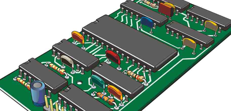
The double panel is a medium layer in the middle, and both sides are wire layers. Multilayer board is multi-layer wire layer, between each two layers is the medium layer, the medium layer can be made very thin. A multilayer circuit board has at least three conducting layers, two of which are on the outer surface, while the remaining layer is synthesized within the insulating board. The electrical connection between them is usually achieved by plated through holes in the cross-section of the circuit board.
When designing a four-layer PCB circuit board, how to design the layering in general?
In theory, there are three options.
In Scheme one, 1 power layer, 1 stratum and 2 signal layers are arranged as follows: TOP (signal layer), L2(stratum), L3(power layer), BOT (signal layer).
In Scheme 2, 1 power layer, 1 stratum and 2 signal layers are arranged as follows: TOP (power layer), L2(signal layer), L3(signal layer), BOT (stratum).
Scheme 3:1 power layer, 1 stratum and 2 signal layers are arranged as follows: TOP (signal layer), L2(power layer), L3(stratum), BOT (signal layer).
Signal layer
stratum
Power layer
Signal layer
What are the pros and cons of each of these three options?
Scheme 1, the main laminated design scheme of the four-layer PCB in this scheme, there is a ground plane under the component surface, and the key signal is preferably distributed in the TOP layer; As for the layer thickness setting, there are the following suggestions: Should the impedance control core board (GND to POWER) not be too thick to reduce the power supply? The distributed impedance of ground plane; * The effect of removing lotus root from the power plane.
Scheme two, some schemes mainly in order to achieve a certain shielding effect, the power supply? Is the ground level on TOP? BOTTOM layer, but in order to achieve the ideal shielding effect, there are at least the following defects :1. Power supply? If the ground distance is too far, the power plane impedance is large. 2. Power supply? The ground plane is incomplete due to the influence of the element pad. As the reference surface is incomplete and the signal impedance is discontinuous, in fact, due to the large number of surface attached devices, the power supply of this scheme is more and more dense for the devices. Ground can hardly be used as a complete reference plane, and the expected shielding effect is difficult to achieve. Option 2 is limited in scope? But in individual veneers, scheme 2 is a better arrangement scheme? Scheme 3: Similar to Scheme 1, this scheme is suitable for the layout of main devices in the BOTTOM or the bottom wiring of key signals;
In the era of industrialization surplus, circuit board manufacturers in particular, choose a suitable circuit board manufacturers is very important! In the industry, large companies such as Shennan, Shenlian and Jingwang are doing well. Their positioning is clear and their customer groups are very stable. Generally, they do not accept factory orders, because they are not short of orders at all.

However, most of the factories in the industry are not clearly positioned, what single is accepted, the result of what single is not good! Do not do well does not matter, reposition, do fine do special as a way out. But most of the boss don't think so, we think they pick up not only, because their strength is not enough, not enough equipment......
In fact, regardless of the size of the market, sometimes operating quality is more important than operating scale! PCB market is very big, you focus on a certain field, do fine, still can be bigger and stronger!
Shenzhen Fanyi Technology Development Co., Ltd. is such a circuit board company! We focus on connector RJ45Type C field for more than ten years, research RJ45 PCB board and Type C PCB board manufacturing difficulties, in 2007, there is no computer V-CUT period, can control the V-CUT tolerance within +/-0.15mm. When everyone thinks the single side welding ring ** meets 0.3mm, they have achieved 0.05mm!
Therefore, PCB proofing, production which good? Of course, choose Dongguan Qixiang Electronic Co., LTD., because Qixiang circuit has a team to study the inherent characteristics of each electronic industry products, according to the characteristics of different products, different production processes.
At present, there are too many circuit board factories and they are very miscellaneous. Electronic manufacturers to choose a wide range, and it is difficult to choose the right manufacturers. A little mistake, mismatched Circuit board manufacturers will bring you a lot of annoyance, and even fatal functional problems, let you not hurt! Of course, the circuit board manufacturers are also many, such as Shennan, Shenlian, Jingwang these big factories, but the general large, Circuit board factory is not just a factory, it is already a platform! It is not short of orders, will not choose to cooperate with you!


Достаточно загрузить файлы Gerber, BOM и проектные документы, и команда KINGFORD предоставит полное предложение в течение 24 часов.