
Контрактное производство электроники под ключ в Китае
Шэньчжэнь, район Баоань, улица Фуюн, улица Фуцяо, район 3, промышленный парк Лонгхуй 6

The miniaturization of electronic components and the application of SMT technology and equipment in electronic products all mark the rapid development of modern science and technology. SMT manufacturing equipment has the characteristics of full automation, high precision and high speed. With the improvement of the degree of automation, higher requirements are put forward for PCB design. PCB design must meet the requirements of SMT equipment, otherwise it will affect the production efficiency and quality, and may even be unable to complete automatic SMT by computer.
PCB design elements affecting SMT manufacturing
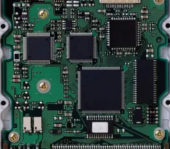
PCB design is a key link in SMT technology, and SMT technology is an important factor to determine SMT manufacturing quality. This paper will analyze PCB design elements that affect the quality of SMT equipment from the perspective of manufacturing. The PCB design requirements of SMT manufacturing equipment mainly include: PCB pattern, size, positioning hole, clamping edge, MARK, panel wiring, etc.
PCB pattern
In SMT automatic production lines, PCB production starts with the loader and is completed through printing, chip installation and welding. Finally, the unloader will produce the finished plate. In this process, the PCB is transmitted along the device path, which requires that the PCB pattern should be consistent with the path transmission between the devices.
PCB size
PCB design size must conform to the maximum and minimum size requirements of the SMT machine. So far, most devices are in the 50mmx50mm to 330mmx250mm (or 410mmx360mm) range.
If the PCB thickness is too thin, the design size should not be too large. Otherwise, the reflux temperature will cause PCB deformation. The ideal aspect ratio is 3:2 or 4:3.
If the PCB size is less than the minimum size requirements of the equipment, the board should be assembled. The number of panels depends on the size and thickness of the PCB.
PCB positioning hole
SMT positioning methods are classified into two types: positioning holes and edge positions and edge positions. However, the most common method of positioning is Mark point counterpoint.
PCB blanking
Because the PCB is transmitted along the path of the device, the component must not be placed in the direction of the gripper edge, or the component will be squeezed by the device, affecting the installation of the chip.
mark
The PCB mark is a point of identification and location for all fully automatic equipment used to correct PCB manufacturing errors.
Shape: square, triangle, solid circle, hollow circle, oval, diamond, cross, etc. One of the first choices is a solid circle.
1. Size: The size must be within the range of 0.5mm to 3mm. A solid circle with a diameter of 1mm is preferred.
2. Surface: The surface is the same as the welding plane of PCB welding pad, and the welding plane is uniform, neither thick nor thin, and the reflection effect is excellent.
A no-go area shall be placed around the Mark point and other pads, which shall not contain screen printing and solder resistance layers.
Silk screen characters and silk screen lines are arranged around the MARK, which will affect the device's recognition of the MARK point, and will cause frequent alarm due to MARK recognition, which seriously affects the manufacturing efficiency.
Splice method
The purpose of combining multiple small PCB of the same or different shapes to form panels is to improve manufacturing efficiency. For some PCB dual board, it is possible to design the top and bottom as one panel so that templates can be made, thus reducing costs. This approach also helps reduce top and bottom movement time, which improves manufacturing efficiency and equipment utilization.
A requirement of the V-groove connection method is to keep the rest of the board (uncut) equal to one quarter to one third of the thickness of the board. If too much circuit board is cut away, the slots may break due to the high temperature of reflow, causing the PCB to fall off, and the PCB will burn in the reflow furnace.
PCB design technology has the characteristics of complex, efficient and strict, this technology must consider the device requirements and device layout, pad design and circuit design. Excellent PCB design is an important factor to ensure product quality. This paper puts forward some problems which should be considered in PCB design from SMT manufacturing point of view. As long as we pay enough attention to these problems, automatic SMT manufacturing of SMT components can be realized
Pcb sharing
2023-03-21


Достаточно загрузить файлы Gerber, BOM и проектные документы, и команда KINGFORD предоставит полное предложение в течение 24 часов.