
Контрактное производство электроники под ключ в Китае
Шэньчжэнь, район Баоань, улица Фуюн, улица Фуцяо, район 3, промышленный парк Лонгхуй 6

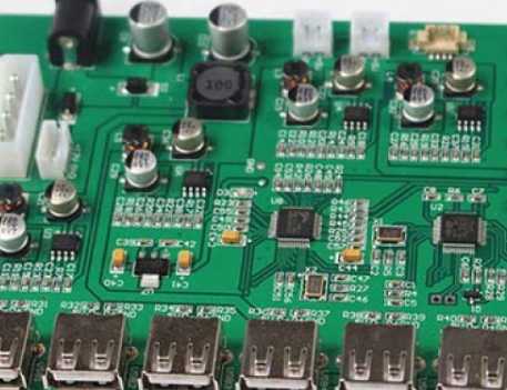
Shenzhen kingford is a professional PCBA manufacturer with its own PCB board factory and SMT patch processing factory. We can provide PCB design, PCB board making, component purchasing, SMT patch, DIP plug-in, PCBA testing, finished product assembly and other one-stop PCBA processing services. Next introduce the four steps of circuit board processing.
First, solder paste stage
1.1 Solder paste
Solder paste (or solder paste) is the key material for welding. As Wikipedia, it is a material used in the manufacturing process of printed circuit boards to attach surface mount components to pads on the board." The paste is initially sticky, heated and attached to the components on the PCB board (following a strict temperature curve), it melts and then solidifies to form an electrical connection.
Solder paste
1.2 PCB Template
A PCB template is a sheet of steel (also known as steel mesh) with many holes in it. The holes are cut by a laser to allow the solder paste to flow.
PCB template
1.3 Solder paste printing press
During the pasting process, we need to make sure that the template holes are aligned with the corresponding pads, and then brush the screams to ensure that all pads can be attached to the screams. Sure, you can paste squeals by hand, but that won't work on hundreds of boards, which is why a solder paste press is needed.
Two, automatic component placement
After the solder squeals on the printed circuit board, the next step is to put the electronics on the bare board.
2.1 Patch machine
SMT machine is the key equipment in Circuit board assembly production, it determines the quality and speed of products, but also determines the maximum production capacity of products. Basically, it is used to "pick up components and put them in the right place".
The engineer will first install all the required components such as resistors/capacitors/IC/connectors etc. in special locations on the machine and then program the patch machine to tell it "Hey, put this resistor/capacitor here".
The key specification for a patch machine is how accurate it can be. In the picture, the patch machine we used is SM481-PIUS, which can handle resistance/capacitor 0201 packages and 0.3mm BGA IC.
2.2 Vacuum Compressor
The patch machine works with a vacuum compressor that pulls the back of the component through a tiny nozzle, so typically, you'll see dozens of nozzles in the machine.
For PCBA prototype/small lot assembly, the most time costly process is component installation/programming and commissioning, which is why a project has a start-up fee, while the unit welding fee is reduced from 10 to 50.
2.3 Gluing machine
Sometimes a PCB has components on both sides, and when one side is welded, the components on the other side may fall off, especially if the components are heavy or larger. The glue machine applies the glue on the PCB board, so that the components sit firmly on the PCB board. This is important for wave soldering, where the force of the welding wave may displace larger elements, or for double-sided wave soldering or reflow soldering to prevent elements from falling off.
Three, reflow welding
3.1 Reflow furnace
Typically, reflow welding is used for surface mount components. After placing the components on bare plates, they are heated by a machine called a reflow furnace
The PCB board on which the component is placed is placed into the machine from one end. On a double-track conveyor belt, the board of the newly placed component is passed through the hot and cold zones of the reflow furnace (most SMT plants have 10 zones). The melting and cooling of the solder is precisely controlled to fill the solder joints. The solder paste is melted and hardened to form an electrical connection. When the PCBA board reaches the other end, the connection becomes strong.
The board was hot when it came out of the machine, so gloves were needed to pick it up.

3.2 Temperature curve of reflow welding
The temperature curve associated with reflow welding is the most important parameter to ensure proper connection of parts. The main temperature changes associated with the reflow welding temperature curve can be divided into four stages/regions
3.2.1 Preheating
The preheating zone is to vaporize the lower melting solvent in the solder paste. The preheating zone needs volatile solvent, but the heating slope must be controlled.
3.2.2 Constant heating
The setting of constant temperature zone is mainly controlled within the parameters of solder paste supplier and the heat capacity of PCB. At this stage, the printed circuit board reaches an even temperature and the flux in the solder paste begins to react positively, thus increasing the wettability.
3.2.3 High-temperature welding
In this region, a complete melting and wetting reaction occurs. This part of the process also needs to be carefully controlled so that the slopes of the temperature rise and fall do not expose the components to thermal shock. The ideal temperature and time in this area are generally 220 ~ 260 degrees, 30s ~ 60s.
3.2.4 Cooling
During cooling, the temperature drops and the solder screeches solidify again. It plays a key role in the final result of the weld. Too slow cooling will cause parts to rise, solder joints to darken or uneven solder joints, while rapid cooling will cause thermal shock to parts.
The setting of the temperature curve is most important for experienced SMT engineers and there are many factors to consider, depending on the PCBA and component, including:
* The maximum temperature the component can withstand. For example, if there is ws2812 on the board, Makerfabs recommends no more than 220 degrees, as we suggested: why does WS2812 SK6812 malfunction after SMT welding.
* Solder paste used. Different creams may require different temperature curves.
* Maximum component size/maximum Pin number. For example, if they are a high-power sensor, the temperature needs to be higher to ensure that the solder paste melts completely.
* PCB temperature specifications
Iv. Inspection and testing
4.1 AOI (Automatic Optical Detection)
There, you can't guarantee that all the components are soldered properly due to many reasons such as component missing/lifting/cold connection... AOI is used to detect these common problems.
The AOI machine uses an optical method to detect defects, which uses a high-definition camera to capture the surface of the circuit board and build up an image of it for analysis. The captured images are then compared to those of the correct reference board to identify various defects, including incorrect components, missing components, cold connections, and so on.
4.2 Programming Tools
For functional testing, especially the controller board, you need some programming tools or burn/write tools, such as Jlink/ offline downloaders, etc.
As an important part of production, it is necessary to master the programming experience of the following chips and be proficient in the use of programming tools and related software.
* PIC chip
* ATMEL series
* ARM series
* Arduino bootstrap program and sketches
* FPGA
* MicroPython is related to Circuit Python
* STM series
* ESP/ESP32 series
4.3 Test Fixture
Functional testing is a critical step to ensure that the final PCBA board works as expected. While physical defects like solder Bridges or tombstones make PCBA "should work," functional tests make the board "ready to go."
As a PCB Assembly plant, it is difficult or impossible to know how a customer's boards are supposed to work. It usually takes a PCBA designer to go through the detailed testing steps and how to tell if the board is working properly.
For users, factory testing of test boards is often very helpful.
A test fixture is made up of a number of needles that are used to contact the pads on the PCBA, so the tester can program and test the pads if they work as expected. Of course, the firmware/software is loaded before making the PCBA board work.
4.4 Visual examination
Yes, this is the last step before packing. After completing all the machine steps, the most basic/simple visual inspection is required to check for any scars/special customer needs and any other problems that the machine cannot detect.
Why do you choose kingford to manufacture circuit boards?
1. Strength guarantee
▪SMT workshop: We have imported SMT machines and several sets of optical inspection equipment, with a daily output of 4 million. Each process is equipped with QC personnel, who can keep an eye on product quality.
▪DIP production line: We have two wave-soldering machines, among which there are more than 10 old employees who have worked for more than three years. The skilled workers can weld all kinds of plug-in materials.
2. Quality assurance, cost-effective
▪ High-end equipment can stick precision shaped parts, BGA, QFN, 0201 materials. Can also template patch, loose material hand.
▪ Sample and size batch can be produced, proofing from 800 yuan, batch 0.008 yuan/point, no start-up fee.
3. Rich experience in SMT and welding of electronic products, stable delivery
▪ Accumulated SMT SMT processing services for thousands of electronic enterprises, involving many kinds of automotive equipment and industrial control motherboard. The products are often exported to Europe and the United States, and the quality can be affirmed by new and old customers.
▪ On time delivery, normal 3-5 days after complete materials, small batch can also be expedited on the same day shipment.
4. Strong maintenance ability and perfect after-sales service
▪ Experienced maintenance engineers can repair all kinds of patch welding caused by bad products, to ensure the connection rate of each piece of circuit board.
▪ 24-hour customer service staff at any time response, the fastest speed to solve your order problems.
How to calculate the cost of PCB copy board?
2023-03-16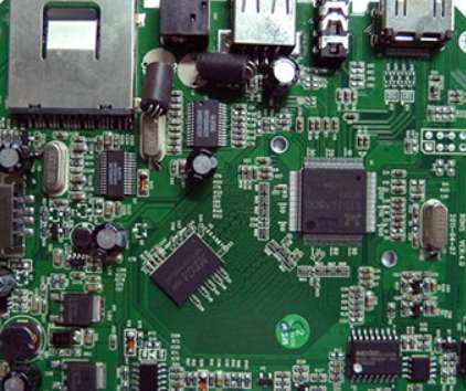


Достаточно загрузить файлы Gerber, BOM и проектные документы, и команда KINGFORD предоставит полное предложение в течение 24 часов.