
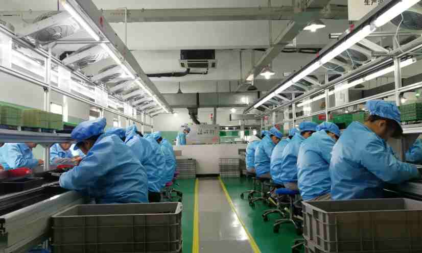
Контрактное производство электроники под ключ в Китае
Шэньчжэнь, район Баоань, улица Фуюн, улица Фуцяо, район 3, промышленный парк Лонгхуй 6

Yesterday we argued about the number of PCB board layers, today we specially consulted the development colleagues, learn from now to sell, share some knowledge with you.
1, what is the structure of PCB board and printed circuit board can be generally divided into two parts, that is, the base material part (generally using good insulation, not easy to bend engineering plastics) and line layer part, which line layer part of the use of conductive medium is copper foil, also called copper skin, copper cover in the entire base two outer surface. This layer is the core of the entire PCB. After the circuit is designed by various design software, special machines will carve the copper foil layer according to the design drawings and carve off the unnecessary parts, thus forming a complete circuit. At the same time, various components (chips, resistors, capacitors, inductors, plugs, fuses, etc.) will be welded or affixed to the PCB, so that it is together with the copper foil layer. To form a complete circuit.
2, what is the layering of PCB board in general, PCB board has two layers, respectively located on the upper and lower surface of the substrate, the upper and lower two layers of the circuit is different, this is because of the needs of the circuit design and safety considerations, such as the power supply part of the line and the grounding part of the line, generally and circuit layer separated on the layer. And in some special times, for some complex circuits, a layer may not be able to exhaust all the lines or a layer of lines can not achieve the control of the circuit (for example, some components have very fine requirements on impedance), then it is necessary to use multi-layer PCB. Multi-layer PCB is actually the single-layer PCB superimposed together, so that different circuits can be designed on different line layers to meet the needs of complex circuits, the general number of PCB layers is divided into 2 layers, 4 layers, 6 layers, 8 layers, 10 layers and so on.
3. How to distinguish PCB layering It is relatively easy to distinguish whether PCB is multi-layer or not, just by looking at the light and observing whether the parts not covered by copper on the upper and lower surfaces are translucent or not. Because if there are other circuit layers in the middle, then transparency will naturally be very low. Roughly by the naked eye to distinguish PCB is several layers, for some senior developers is also possible ~ but accurately judge is several layers, is difficult to do.
4. PCB color difference There is no uniform standard for the color of PCB circuit board, so there is no saying that other colors of PCB must be better than green, but in PCB design, green board is the most commonly used, because the green surface does not look harsh, and some manufacturers in order to highlight their own design, The PCB color is often changed on some high-quality products to achieve a different visual effect. Maybe this is the source of the feeling that "other colors are better than green".
5, how to choose PCB circuit board First of all, according to the customer's industry needs to stipulate that PCB is several layers, such as a customer is to do motherboard graphics card circuit board, it is only a small part of the selection, because all the board card in mass production before, will certainly go through the reliability test, even if the use of 4 layers of board or even 2 layers of board, It is also certain that it can meet the requirements of product performance. Moreover, most businesses will not understand the PCB board several layers, so this aspect is not of great significance in the actual purchase, so you can not be too constrained.

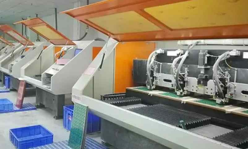
PCB boards are widely used in the field of automatic testing of printed circuit boards
To understand the PCB board machine to establish the relevant application software, using the idea of virtual instrument, that is, through the software to achieve a variety of functions of traditional instruments, including oscilloscope, signal generator, and a variety of mathematical processing of data acquisition. During the test, the digital signal is given through the test software. PCB board test system will have a new design idea, the use of automatic test system based on USB bus and virtual instrument design idea, give full play to the role of the computer, as far as possible by the computer to replace the idea of traditional instruments, thus reducing the volume of the instrument itself, reduce the development cost, so as to improve the efficiency of development.
After D/A conversion, the simulated excitation signal required by the test is applied to the test system, and then the test circuit is sent to the switch matrix through the test bus. When the switch matrix is connected with it, it is controlled by the microprocessor. The PCB board under test is fixed on the needle bed, and the excitation signal is applied to the corresponding position of the printed circuit board, and its response is measured by the test circuit. The analog quantity collected is sent into the core control, and the corresponding digital quantity is obtained after A/D conversion. The software on PCB is fed back and processed by PCB to determine whether the PCB board is qualified. The online testing technology has broken through the previous method of using human eyes to detect the circuit board. The online testing technology has high efficiency, low detection rate, and realized the automation of the detection field. The detection system adopts the idea of combining with virtual instrument, reducing the hardware design and reducing the cost of the whole system.
The basic method of PCB board analog components online test and diode, triode test method, this test system is suitable for the application of small and medium enterprises. It reduces the number of unqualified products entering the next process, thus reducing the amount of rework of products, improving production efficiency, reducing the total cost of manufacturing, and improving the profits of enterprises. It is a detection technology widely used at present, and it is an efficient, high-speed and high-precision detection method. At present, PCB board is widely used in the field of automatic testing of printed circuit board, including the testing of uninstalled components and installed components. Currently, the commonly used test methods are: on-off testing, in-circuit testing, functional testing, edge testing, optical testing and X-ray testing. Online testing is based on the specific characteristics of PCB board, select the appropriate detection method to combine one or more processes together, learn from each other, comprehensive application.


Достаточно загрузить файлы Gerber, BOM и проектные документы, и команда KINGFORD предоставит полное предложение в течение 24 часов.