
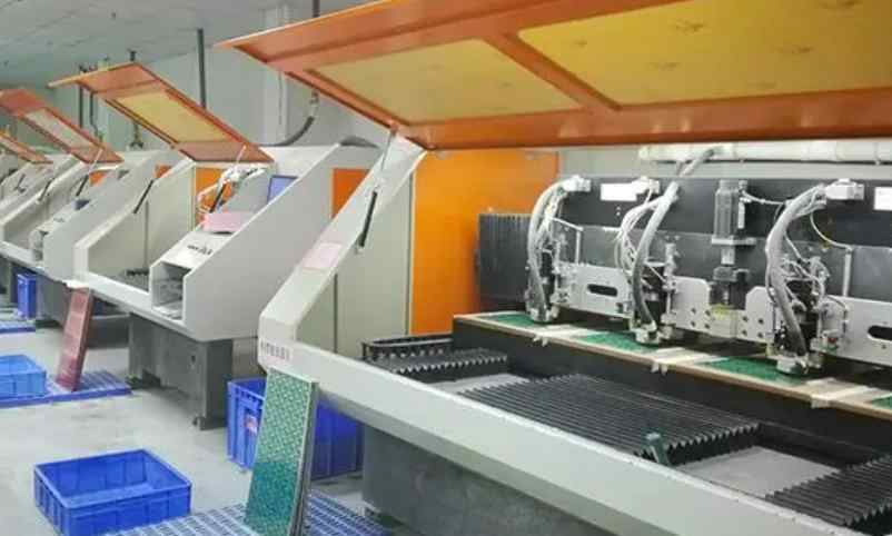
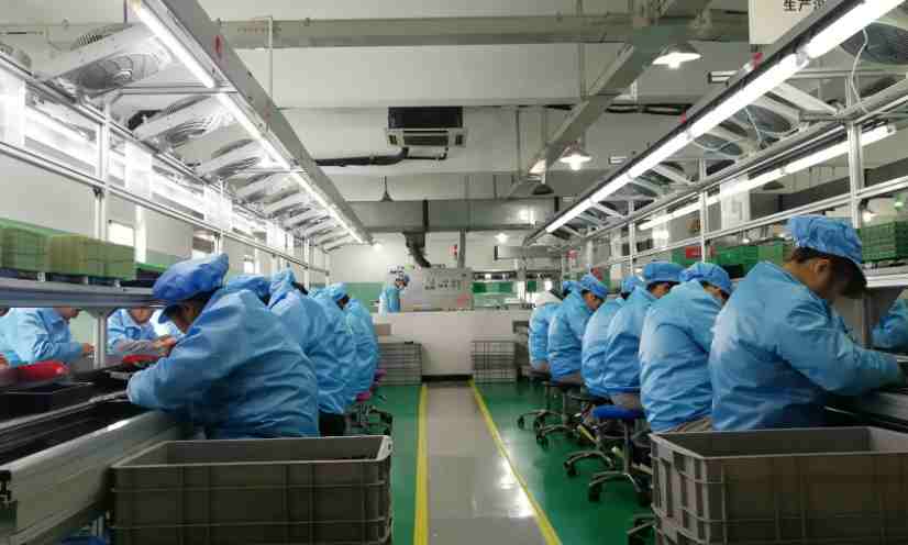
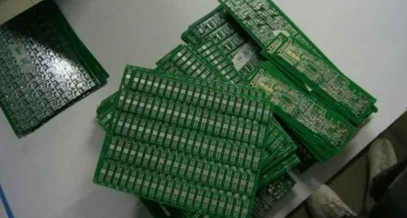
Контрактное производство электроники под ключ в Китае
Шэньчжэнь, район Баоань, улица Фуюн, улица Фуцяо, район 3, промышленный парк Лонгхуй 6

1.3 Wires above the point shall pass through each point in turn as far as possible, so as to facilitate the test. The length of the line shall be as short as possible.
2. The hole should be coated with green oil (set to negative one time value).
3. The lines between different layers should not be parallel to avoid the formation of actual capacitance.
4. Wiring is as straight as possible, or 45 degrees broken line, to avoid electromagnetic radiation.
5. Ground and power cables should be at least 10-15mil (for logic circuits).
6. It is better not to place PAD or over empty under the battery holder. Pad and VIL are of reasonable size.
7. Consider more reinforcement, hollowed out components and other ways to avoid excessive radiation sources.
8. Function block components should be put together as far as possible. Components near LCD such as zebra strips should not be too close.
9. Try not to release cables between pins, especially between and around integrated circuit pins.
10. Connect the multisense cables to increase the ground area. Line to line as neatly as possible.
11. The structure of component emission should be considered. Positive and negative electrodes of patch components should be marked in packaging and at the end to avoid space conflict.
12. The oscillating circuit element should be as close to IC as possible, and the oscillating circuit should be as far away from the antenna and other areas prone to interference as possible. Ground pad should be placed under crystal vibration.
13. After wiring is complete, carefully check that each connection (including NETLABLE) is actually connected (using the lighting method).
14. Currently printed boardscan be used for 4-5mil wiring, but usually used for 6mil line width, 8mil line spacing, 12/20mil pad. Wiring should consider the influence of filling current, etc.
15. Pay attention to uniform component discharge, so as to facilitate installation, plug-in, welding operation. Text emission in the current character layer, reasonable position, pay attention to the orientation, avoid being blocked, easy to produce.
16. Design process: A: design schematic diagram; B: Confirm the principle; C: Check whether the electrical connection is complete; D: Check whether all components are packaged and whether the size is correct; E: Place components; F: Check whether the component position is reasonable (printable 1); G: Ground wire and power cord can be distributed first; H: Check whether there is a flying line (other layers except the flying line layer can be turned off); I: Optimize wiring; J: Check the wiring integrity again; K: Compare the network table to check whether there is any omission; L: Rule check, there is undeserved error label; M: text description arrangement; N: Add the symbol of the board description; O: Comprehensive inspection.
 LED aluminum substrate is a very important "character" in LED lighting.
The most remarkable feature of the e-profession is that it is constantly changing, and the skills of the e-profession are constantly updated. In our daily life, we come into contact with the high-tech LED aluminum substrate raw materials. The earliest use is always electronic products, and electronic products have been updated at a very fast speed.
LED technology is now not a new technology, but still in everyone's mind to carry on the storm, feel the change brought by the new technology. In LED lighting, there is a very important figure, that is the use of LED aluminum substrate. The use of LED aluminum substrate material is very special. The two sides of the LED aluminum substrate, one is to form the LED current circuit, the demand is very precise technology, the other is the LED aluminum substrate is a very important aspect, constitute a relatively stable cooling system. LED aluminum substrate raw material is such a prominent advantage, as a substrate, copper substrate and iron substrate are able to think about the raw material, but compared to the performance of the three, it is still better to choose LED aluminum substrate, LED aluminum substrate raw material is relatively speaking, has good plastic function, but also has good heat dissipation effect, is a very suitable material, First, the cost will not be too high.
LED aluminum substrate raw materials because of its excellent heat dissipation effect, make the heat dissipation in the circuit process timely evaporation, prolong the service life of components, but also make the circuit more stable and durable. Keyou Circuit is a professional production of high precision multilayer circuit board, module gold circuit board, vehicle circuit board, traffic recorder,COB power supply, computer motherboard, medical circuit board, module Bonding board, thermoelectric separation copper substrate, etc., quality assurance, delivery on time, to sales as one of the high-tech enterprises.


Достаточно загрузить файлы Gerber, BOM и проектные документы, и команда KINGFORD предоставит полное предложение в течение 24 часов.