
Контрактное производство электроники под ключ в Китае
Шэньчжэнь, район Баоань, улица Фуюн, улица Фуцяо, район 3, промышленный парк Лонгхуй 6


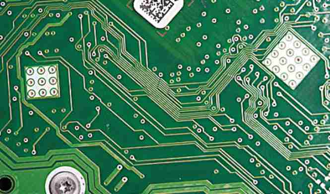
1. Because the crystal structure formed by sinking gold and gold-plating is different, sinking gold is easier to weld than gold-plating, and will not cause poor welding and cause customer complaints.
2. Because of the different crystal structure formed by sinking gold and gold plating, sinking gold will be more yellow than gold plating, and customers are more satisfied.
3. Because of the denser crystal structure of gold plating, it is not easy to produce oxidation.
4. Because the gold plating only has nickel gold on the pad, the signal transmission in the skin effect is in the copper layer, which will not affect the signal.
5, because the gold plate only has nickel gold on the welding plate, so the welding resistance on the line and the combination of copper layer is more firm.
6, because the gold plate only has nickel gold on the pad, so it will not be produced into gold wire caused by short.
7, because of the gold and gold plating formed by the crystal structure is not the same, the stress of the gold plate is easier to control, for the products of the state, more conducive to the processing of the state. At the same time, because the gold is softer than the gold, so the gold plate is not wear-resistant gold finger.
8, the project will not affect the spacing when making compensation.
9. The flatness and service life of the gold plate are as good as that of the gold plate.
Keyou Circuit Technology Co., Ltd. was founded in 2003, is committed to PCB proofing and mass production, with high precision single side/double side/multilayer circuit board (1-26 layers), thermoelectric separation copper substrate, multilayer industrial circuit board, power PCB board, medical circuit board, security PCB board, communication PCB board, automotive circuit board, Instrument circuit board, military circuit board, composite bus copper substrate, foldable metal substrate, FPC soft and hard combined board, quality assurance, delivery on time, to sales as one of the high-tech enterprises.

LED sensors for wearable fitness devices
More and more people are tracking their physical fitness through wearable gadgets and appropriate apps. Optical sensors are suitable for measuring pulse rate and oxygen saturation. Already well established in the medical field, this technology can now be transferred to consumer applications thanks to modern LED technology. All of this can be traced back to the bracelet that keeps track of people's steps. Now, various activity trackers, such as fitness bands and smartwatches, can also measure heart rate and other biological indicators or monitor sleep quality. Many people are excited about the new opportunity to track their fitness levels, giving rise to the growing popularity of the "quantified self" movement.
Big players like Samsung, Apple and Google are entering this growing market with the right apps, smartwatches and smartphones, and while pedometers use acceleration sensors, optical methods commonly used in the medical field to measure pulse and blood oxygen are making their way into the consumer market. In hospital Settings, sensors are mostly mounted in ear or finger clips. In 2013, Mio Alpha's smartwatch became the first wristband product to use optical sensors to measure pulse rate on the wrist -- a significant improvement over the chest straps worn by athletes, which no one wants to wear all day. A smartphone can also be used to measure pulse rate on a finger. The first fitness bands, which measure oxygen saturation in your blood simply by placing your finger on a screen, are now entering the market. This feature is useful for people who work at high altitudes, such as mountaineers, skygliders and glider guides, as well as people with heart or lung diseases
How can PCB control the quality of copper plating layer
It is very important to control the quality of electroplating copper layer of through-hole printed circuit board. Because the development of multilayer or laminated board to high density, high precision and multi-function direction, the requirements of binding force, uniform fineness, tensile strength and elongation of copper plating layer are more and more strict, and also more and more high, so the quality control of through-hole printed circuit board electroplating is particularly important. Keyou Circuit is committed to PCB proofing and mass production, with high precision single side/double side/multilayer circuit board (1-26 layers), thermoelectric separation copper substrate, multilayer industrial circuit board, power pcb board, medical circuit board, security PCB board, communication PC board, automotive circuit board, instrument circuit board, military circuit board, composite bus copper substrate, Foldable metal substrate, FPC soft and hard combined board, quality assurance, delivery on time, to sales as one of the high-tech enterprises.
Ensure the uniformity and consistency of the copper plating layer of through-hole printed circuit board. In the process of copper plating of printed circuit board with high aspect ratio, most of them are carried out under the auxiliary action of high-quality additives, with moderate air stirring and cathode movement, under the condition of relatively low current density, so that the electrode reaction control area in the hole is enlarged.
The role of plating additives can be shown, coupled with the cathode movement is very conducive to the plating solution of deep plating ability to improve, increase the polarization of plating parts, electrocrystallization process of the coating nucleation rate and grain growth rate compensation each other, so as to obtain high toughness copper layer. Of course, the current density is set according to the actual plating area of the printed circuit board being plated. From the analysis of the original understanding of electroplating, the value of current density must also depend on the main salt concentration of high acid and low copper electrolyte, solution temperature, additive content, stirring degree and other factors. In short, the technological parameters and conditions of copper plating must be strictly controlled to ensure that the thickness of the copper plating layer in the hole meets the requirements of the technical standard.


Достаточно загрузить файлы Gerber, BOM и проектные документы, и команда KINGFORD предоставит полное предложение в течение 24 часов.