
Контрактное производство электроники под ключ в Китае
Шэньчжэнь, район Баоань, улица Фуюн, улица Фуцяо, район 3, промышленный парк Лонгхуй 6

Three anti paint is a special formulation of paint, used to protect circuit boards and related equipment from environmental erosion. Three anti paint has good high and low temperature resistance; After curing, it forms a transparent protective film, which can protect the circuit from damage under conditions such as vibration, moisture, salt spray, humidity and high temperature containing chemical substances (e.g. fuel, coolant, etc.). Under these conditions, the circuit board may be corroded, mold growth and short circuit, etc., with superior insulation, moisture-proof, anti-leakage, dustproof, anti-corrosion, anti-aging, anti-mildew, anti-loosening parts and insulation resistance to corona and other properties.
Three anti paint effect
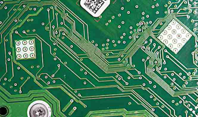
Moisture is the most prevalent and destructive major factor on PCB boards. Excessive moisture will greatly reduce the insulation resistance between conductors, accelerate high speed decomposition, reduce Q value, and corrode conductors. We often see PCB circuit board metal part of the patina is not coated with three anti-paint metal copper and water vapor, oxygen caused by the chemical reaction.
The three-proof paint is applied to the printed circuit board and components to reduce or eliminate the performance degradation of electronic products when they may be affected by adverse factors in the operating environment. If the three anti paint can maintain its function for a satisfactory period of time, such as longer than the life of the product, it can be considered to have achieved its coating purpose.
Three anti-paint components
Acrylic products
Acrylic three anti - paint flexibility can provide comprehensive protection. Because it is a single component system, with good adhesion, simple operation, not high requirements for equipment and conditions, convenient construction, high transparency, high brightness, short operation cycle and other characteristics, so they are easy to use and easy to clear. Some acrylic products meet military standards. They dry quickly and do not melt. They can be cleaned up with an accompanying organic solvent, so these circuit boards are one of the most versatile and effective products on the market.

Is three anti paint toxic
Three anti-paint toxic depends on the use of three anti-paint thinner and solvent type, if three anti-paint use toluene, xylene as diluent, this chemical is harmful to human health, if the use of lipids, alcohols and other less harmful. Xylene is moderately toxic, irritating to the eyes and upper respiratory tract. In high concentrations, xylene has anesthetic effects on the central system.
Although there are many so-called environmental protection three anti-paint on the market, but in actual use, we are still necessary to take protective measures, wear gas masks when using.
Eight kinds of PCB surface treatment technology
With the continuous improvement of human requirements for living environment, the environmental problems involved in PCB production are particularly prominent. The topic of lead and bromine is the hottest, lead-free and halogen-free will affect the development of PCB in many ways. Miss LAN Although at present, the change in PCB surface treatment technology is not very big, it seems to be a relatively distant thing, but it should be noted that the long-term slow change will lead to great changes. In the case of environmental protection increasingly loud voice, PCB surface treatment technology will definitely change in the future. The most basic purpose of surface treatment is to ensure good solderability or electrical properties.
Since natural copper tends to exist in the form of oxides in the air, it is unlikely to remain as raw copper for a long time, so other treatments are required for copper. Although strong flux can be used to remove most copper oxides in subsequent assembly, strong flux itself is not easily removed, so it is generally not used in the industry. There are many PCB surface treatment processes. The common ones are hot air finishing, organic coating, electroless nickel plating/gold dipping, silver dipping and tin dipping, which are described below.
1, hot air leveling (tin spraying) Hot air leveling, also known as hot air solder leveling (commonly known as tin spraying), it is in the PCB surface coated with molten tin (lead) solder and heating compressed air leveling (blowing) process, so that it forms a layer of copper oxidation resistance, but also can provide good solderability coating layer. Hot air conditioning solder and copper at the joint of the formation of copper tin gold compounds.PCB for hot air polishing usually to sink in the molten solder; The air knife blows out the liquid solder before it sets; The air knife minimizes the meniscus of solder on the copper surface and prevents solder bridging.
2, organic weldability protection agent (OSP) OSP is printed circuit board (PCB) copper foil surface treatment in line with the requirements of the RoHS directive of a process. OSP is short for Organic Solderability Preservatives, also known as organic solderability preservatives and Preflux in English. Simply put, OSP is a chemically grown organic skin film on a clean, bare copper surface. This layer of film has anti-oxidation, heat shock, moisture resistance, to protect the surface of copper in the normal environment no longer continue to rust (oxidation or vulcanization, etc.); But in the subsequent welding high temperature, this protective film must be easily removed by the flux quickly, so that the exposed clean copper surface can be immediately combined with the molten solder in a very short time to become a solid solder spot.
3, full plate nickel plating gold plate nickel plating is in the PCB surface conductor first coated with a layer of nickel and then coated with a layer of gold, nickel plating is mainly to prevent the diffusion between gold and copper. There are two types of electroplated nickel gold: soft gold plating (pure gold, the surface of gold does not look bright) and hard gold plating (smooth and hard surface, wear-resistant, containing cobalt and other elements, the surface of gold looks brighter). Soft gold is mainly used in chip packaging gold wire; Hard gold is mainly used for electrical interconnection in non-welded places.
4. Gold plating is wrapped in a thick layer of nickel gold alloy with good electrical properties on the copper surface, which can protect PCB for a long time; In addition, it has environmental tolerance that other surface treatment processes do not have. Sinking gold also prevents copper from dissolving, which would help lead-free assembly.
5. Sunk tin Because all solder is currently based on tin, so the tin layer can match any type of solder. Tin sinking process can form flat copper-tin intermetallic compounds. This property makes tin sinking have the same good solderability as hot air leveling without the headache flat problem of hot air leveling. The tin plate cannot be stored for too long and must be assembled according to the order of the tin sinking.
6, silver plating process is between organic coating and electroless nickel plating/gold plating, the process is relatively simple and fast; Even when exposed to heat, humidity, and pollution, silver is still able to maintain good solderability, but tarnish. Silver plating does not have the good physical strength of electroless nickel/gold plating because there is no nickel underneath the silver layer.
7, chemical nickel and palladium compared with the precipitation of gold in the chemical nickel and palladium is more than a layer of palladium between nickel and gold, palladium can prevent the corrosion phenomenon caused by the replacement reaction, for the precipitation of gold is fully prepared. Gold is closely coated with palladium, providing a good contact surface.
8, electroplating hard gold plate in order to improve the wear resistance of the product, increase the number of inserting and pulling and electroplating hard gold. With more and more high requirements of users, environmental requirements are more and more strict, surface treatment process is more and more, in the end the choice of the kind of development prospects, more universal surface treatment process, seems to be a little dazzling, confusing. It is impossible to predict exactly where PCB surface treatment technology will go in the future. Anyway, to meet the requirements of users and protect the environment must be done first!


Достаточно загрузить файлы Gerber, BOM и проектные документы, и команда KINGFORD предоставит полное предложение в течение 24 часов.