
Контрактное производство электроники под ключ в Китае
Шэньчжэнь, район Баоань, улица Фуюн, улица Фуцяо, район 3, промышленный парк Лонгхуй 6

1. Introduction
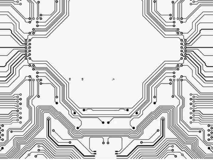
Welding is actually a chemical process. A printed circuit board (PCB) is a support for circuit components and devices in electronic products. It provides electrical connections between circuit components and devices. With the rapid development of electronic technology, PCB density is higher and higher, more and more layered, sometimes all the design may be very correct (such as no damage to the circuit board, printed circuit design is perfect, etc.), but due to the problems in the welding process, resulting in welding defects, welding quality decline thereby affecting the qualified rate of the circuit board, and then lead to the quality of the whole machine is not reliable. Therefore, it is necessary to analyze the factors that affect the welding quality of printed circuit board, analyze the causes of welding defects, and improve the welding quality of the whole circuit board according to these reasons.
How do PCB welding defects cause
2. Causes of welding defects

2.1 PCB design affects welding quality
In the layout, PCB size is too large, although welding is easier to control, but the printing line is long, impedance increases, anti-noise ability decreases, cost increases; After hours, the heat dissipation decreases, welding is not easy to control, easy to appear adjacent lines interference with each other, such as the electromagnetic interference of the circuit board. Therefore, PCB board design must be optimized: (1) shorten the connection between high-frequency components, reduce EMI interference. (2) Large weight (such as more than 20g) components, should be fixed with a support, and then welded. (3) Heat dissipation of the heating element should be considered to prevent defects and rework caused by large ΔT on the surface of the element. The thermal sensitive element should be far away from the heating source. (4) the arrangement of components as parallel as possible, so not only beautiful and easy to weld, suitable for mass production. circuit board design is the best 4∶3 rectangle. Do not mutate the wire width to avoid discontinuity in the wiring. When the circuit board is heated for a long time, copper foil is easy to expand and fall off. Therefore, large area copper foil should be avoided.
2.2 Weldability of circuit board holes affects welding quality
Poor weldability of circuit board holes will produce virtual welding defects, affect the parameters of components in the circuit, lead to the instability of multilayer components and inner wire conduction, and cause the functional failure of the entire circuit. The so-called welderability is the property of the metal surface being wetted by molten solder, that is, the metal surface where the solder forms a layer of relatively uniform continuous smooth adhesion film. The main factors affecting the solderability of printed circuit board are: (1) the composition of solder and the nature of the solder. Solder is an important part of the chemical process of welding. It is composed of chemical materials containing flux. The common low melting point eutectic metal is Sn-Pb or Sn-Pb-Ag. The content of impurities should be controlled by a certain proportion to prevent the oxides produced by impurities from being dissolved by flux. The function of flux is to help solder wet the circuit surface of the plate by transferring heat and removing rust. White rosin and isopropyl alcohol solvents are commonly used. (2) Welding temperature and metal surface cleanliness will also affect the weldability. The temperature is too high, the solder diffusion speed is accelerated, at this time has a high activity, will make the circuit board and solder melt surface rapid oxidation, welding defects, circuit board surface pollution will also affect the weldability resulting in defects, these defects include tin beads, tin balls, open circuit, poor gloss.
2.3 Welding defects caused by warping
PCB and components produce warping in the welding process, resulting in defects such as virtual welding and short circuit due to stress deformation. Warping is often caused by an imbalance in temperature between the upper and lower parts of the PCB. For large PCB, due to the weight of the board falling will also produce warping. Common PBGA devices are about 0.5 mm away from the printed circuit board. If the device on the circuit board is large, the solder joint will be under stress for a long time as the circuit board returns to its normal shape after cooling. If the device is raised 0.1 mm, it will be enough to cause an open weld.
At the same time the PCB produces warping, the component itself may also produce warping, and the solder joint located in the center of the component is lifted away from the PCB, resulting in air welding. This often happens when only flux is used and no solder paste is used to fill the gap. When using solder paste, due to deformation, the solder paste and the welding ball are connected together to form a short circuit defect. Another cause of short circuit is the delamination of the component substrate during backwelding. This defect is characterized by the formation of bubbles under the device due to internal expansion. Under X-ray detection, it can be seen that the welding short circuit is often in the middle of the device.
3. Closing remarks
In summary, by optimizing PCB design, using excellent solder to improve the solderability of circuit board holes and preventing warping to prevent defects, the welding quality of the entire circuit board can be improved.


Достаточно загрузить файлы Gerber, BOM и проектные документы, и команда KINGFORD предоставит полное предложение в течение 24 часов.