
Контрактное производство электроники под ключ в Китае
Шэньчжэнь, район Баоань, улица Фуюн, улица Фуцяо, район 3, промышленный парк Лонгхуй 6

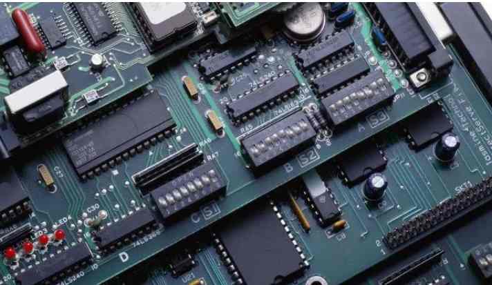
Wiring is the most important process in the whole circuit board design, which will directly affect the performance of the whole product. In the process of circuit board design, wiring is generally divided into three levels: one is cloth tong, which is the most basic requirements of PCB design, if the line is not cloth tong, everywhere is flying line, it is an unqualified circuit board. The second is to meet the electrical performance, which is to measure whether the circuit board qualified standard. This is after the cloth Tong, carefully adjust the wiring, so that it can achieve the best electrical performance. Finally, beauty. If your wiring is well laid, nothing will affect the performance of electrical appliances, but the overall surface looks messy, then electrical performance no matter how good, in the eyes of others is also a design unqualified circuit board, which will bring great inconvenience to the assembly and testing process of circuit board patch processing manufacturers. Wiring should be neat, not crisscross, not disorderly, these are to ensure the performance of electrical appliances and meet the other individual requirements of the condition, otherwise it is a waste of resource investment. Next, by the circuit board patch processing manufacturer -kingford- to explain the basic principles of PCB design and wiring, I hope to help you!
1. In general, the power cord and ground wire should be wired first to ensure the electrical performance of the circuit board. Widen the width of the power supply and ground cable as much as possible. The ground cable should be wider than the power cable. Their relation is ground. Power cord > Signal cable. Generally, the width of signal line is 0.2~0.3mm, and the narrowest width can reach 0.05~0.07mm. The power line is generally 1.2 ~ 2.5mm. For digital circuit PCB, wide ground wire can be used to form a circuit, which can form a ground net for use (analog circuit can not be used in this way).
2, in advance to the requirements of strict line (such as high-frequency line) wiring, input and output side should avoid parallel adjacent, so as to avoid reflection interference. Grounding should be added when necessary, two adjacent layers of wiring to each other vertical, parallel easy to produce parasitic coupling;
3, the oscillator shell is grounded, the clock line should be as short as possible, and can not lead everywhere. Under the clock oscillator circuit, the special high-speed logic circuit should increase the area of the ground, rather than other signal lines, so that the surrounding electric field tends to zero;
4, as far as possible, the use of 45 degrees of polyline wiring, can not use 90 degrees of polyline, in order to reduce the radiation of high frequency signal; (Double arcs are also used for high demand lines);
5, any signal line do not form a loop, if inevitable, the loop should be as small as possible; Signal line holes should be as little as possible;
6, the key line as short and thick as possible, and add protection on both sides;
7. When sensitive signals and noise field signals are transmitted through flat cables, they should be led out by the way of "ground - signal - ground";
8, key signals should be reserved for testing points, in order to facilitate the PCB patch processing and maintenance testing;
9. After schematic wiring is completed, wiring should be optimized. At the same time, after the preliminary network inspection and DRC inspection were correct, the ground wire was filled in the unwired area, and a large area of copper layer was used as the ground wire. On the printed board, the unused places were connected to the ground as the ground wire. Or made of multilayer board, power supply, ground wire each occupy a layer;
The above content is the circuit board patch processing manufacturer -kingford to provide you with (PCB circuit board design and wiring basic principles) related knowledge
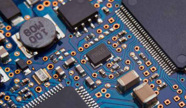
2. How to improve SMT patch processing efficiency?
SMT process is a multi-equipment and multi-process processing sequence. If the connectivity of each process is not strong, even a small mistake may lead to shutdown. It will not only affect SMT patch processing efficiency, but also affect product quality. The production capacity of SMT is also the most important part to drive the operation of the whole factory. Under the premise of ensuring the quality of PCBA welding, if the efficiency of a SMT plant is extremely high, it can also prove the overall strength of the factory. So in such an important process, how can we improve the production efficiency of SMT patch processing? Next, the patch processing manufacturer -kingford- for you to elaborate, I hope to bring you some help!
First, prepare for work in advance
Due to the particularity of PCBA process, SMT must be the first process. At the same time of the first processing procedure, the cooperation degree of various departments is also one of the keys to ensure the SMT patch processing efficiency. Including the accurate output of the entire processing process documents, the accuracy of component procurement, the accuracy of component inspection, material preparation, program editing, solder paste thawing, components baking, etc. These are the preparation of the work in advance, rather than in the actual production process to do or confirm. It can avoid as many problems as possible outside the actual production and processing, which also solves the time of online abnormal processing, and indirectly improves the efficiency of SMT patch processing. Advance preparation work and SMT plant management process has a lot to do with.

2. Ensure the running time balance of SMT mounter
Previously, we talked about the advance preparation of program editing, which is also directly related to the SMT patch processing efficiency. If we understand SMT industry, we will find that the running time of multiple SMT machines in a production line is quite different. Even if it is a few seconds before pasting a piece of PCBA, the production time of the whole order may be several hours or more. So in order to improve production efficiency, when editing the program, the engineer must ensure that multiple installers in a production line run the same time. Reducing downtime waiting time is the most effective way to improve production efficiency.
3. Operation parameters of equipment
When optimizing the mounting program, the synchronization rate of multiple mounting heads absorbing components of the mounting machine should be optimized to the highest, so as to reduce the number of changing the nozzle when the mounting head picks up components and save the mounting time. The feeder with more picks should be placed on the feed station near the printed board. In a pick up cycle, try to only take material from the front or back of the station to reduce the mounting head travel distance. During each pick - up cycle, the mounting head should be fully loaded.
The above content is provided by kingford, Shenzhen SMT processing manufacturer, to learn more about SMT processing knowledge


Достаточно загрузить файлы Gerber, BOM и проектные документы, и команда KINGFORD предоставит полное предложение в течение 24 часов.