
Контрактное производство электроники под ключ в Китае
Шэньчжэнь, район Баоань, улица Фуюн, улица Фуцяо, район 3, промышленный парк Лонгхуй 6

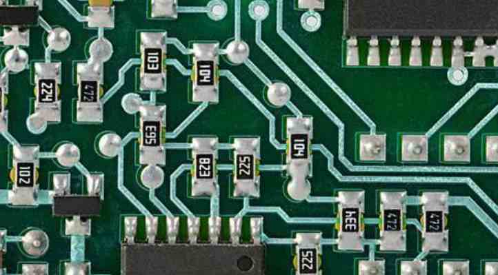
The deformation of the circuit board (PCBA board) usually comes from the rapid temperature rise and rapid temperature drop (thermal expansion and cold contraction) caused by Reflow, coupled with the uneven distribution of parts and copper foil on the circuit board, which worsens the deformation of the circuit board.
 First, the method to increase the circuit board deformation resistance is:
1. Increase the thickness of the PCB board. If possible, you are advised to use a circuit board with a thickness greater than 1.6mm. If you still have to use 0.8mm, 1.0mm, 1.2mm thickness of the board, it is recommended to use the furnace jig to support and strengthen the deformation of the board during the furnace. Although you can try to lower it.
2. Use high Tg PCB material. High Tg means high rigidity, but the price will also go up, this must be a trade-off.
3. Epoxy glue (potted) was applied to the circuit board. You can also consider filling glue around the BGA or on the back of the corresponding circuit board to strengthen its stress resistance.
4. Add reinforcement around the BGA. If there is room, consider building a house with supporting iron frames around the BGA to strengthen its resistance to stress.
2. Reduce the deformation of PCB
Generally speaking, when the circuit board (PCB) is assembled into the case should be protected by the case, but because today's products are thinner and thinner, especially handheld devices, often external bending or falling impact caused by circuit board deformation.
To reduce the deformation caused by external force on the circuit board, there are the following methods:
1. Strengthen the shell to prevent its deformation from affecting the internal circuit board.
2. Add screws or positioning fixing mechanisms around the BGA of the printed circuit board. If our purpose is to protect the BGA, then we can force the mechanism near the BGA to be fixed, so that the BGA near the deformation is not easy.
3. Increase the buffer design of the mechanism on the circuit board. For example, design buffers so that even if the casing is deformed, the circuit board inside will remain unaffected by external stresses. But the life and capacity of the buffer must be considered.
Third, enhance the reliability of BGA
1. underfill the bottom of the BGA.
2. Use the SMD(Solder Mask Designed) layout. Cover the pad with green paint.
3. Increase the amount of solder. But it must be controlled in the absence of short circuit.
4. Increase the size of BGA welding pad on the circuit board. This makes wiring the board difficult because there is less space between the balls for wiring.
5. Design with Vias-in-pad(VIP). But the hole (via) on the welding pad must be electroplated to fill the hole, otherwise there will be bubbles generated when back welding, but it is easy to cause the tin ball to break from the middle. It's like building a house and breaking a pile.
6. I strongly suggest that if it is already finished, it is better to use [Stress Gauge] to find out the stress concentration point of the circuit board. If you have trouble, consider using a computer simulator to see where the possible stresses might be concentrated.
The advantages and disadvantages of the plating process and the plating process of the circuit board?
In the actual trial process, 90% of the gold plate can be replaced by gold-plated plate. The poor weldability of gold-plated plate is its fatal deficiency, which is also the direct reason for many companies to give up gold-plated plate! In the process of use, because of the small conductivity of gold and widely used in contact road, such as keyplate, gold finger plate, gold plate to sink gold plate the most fundamental difference is that gold is hard gold, sink gold is soft gold.
What is gold deposition: through the method of chemical REDOX reaction to generate a layer of coating, generally thicker, is a kind of chemical nickel gold deposit method, can reach a thicker gold layer, usually called gold deposition.
1. The crystal structure formed by sinking gold and gold-plating is different. The thickness of sinking gold is much thicker than that of gold-plating, and sinking gold will be more yellow than gold-plating, and customers are more satisfied.
2, gold plating is more dense crystal structure, not easy to produce oxidation.
3. There is only nickel gold on the solder plate, and the signal transmission in the skin effect is in the copper layer, which will not affect the signal.
4. Only nickel gold is on the solder plate, so the welding resistance on the line is more solid with the copper layer. The work will not affect the spacing when compensating.
5, with the wiring more and more dense, line width, spacing has reached 3-4MIL. Gilding is easy to produce gold wire short circuit. Gold plating only has nickel gold on the pad, so it will not produce gold wire short circuit.
6. The crystal structure formed by sinking gold and gold plating is different. Sinking gold is easier to weld than gold plating, which will not cause poor welding and cause customer complaints. The stress of the sunk gold plate is easier to control, which is more conducive to the processing of the bunding products. At the same time, because the gold is softer than the gold, so the gold plate is not wear-resistant gold finger.
7, generally used for relatively high requirements of the board, the flatness is better, generally the use of gold, gold will not appear after the assembly of the black pad phenomenon. The flatness and service life of the gold plate are as good as those of the gold plate.


Достаточно загрузить файлы Gerber, BOM и проектные документы, и команда KINGFORD предоставит полное предложение в течение 24 часов.