
Контрактное производство электроники под ключ в Китае
Шэньчжэнь, район Баоань, улица Фуюн, улица Фуцяо, район 3, промышленный парк Лонгхуй 6

Copper coating process is very simple, generally can be made by calendering and electrolytic method, the so-called calendering is the high purity (> 99.98%) of copper is pasted on pcb substrate by rolling method. Because epoxy resin has excellent adhesion with copper foil, copper foil has high adhesion strength and working temperature, and can be immersed in molten tin at 260℃ without foaming.
The process is similar to rolling dumpling wrappers, which can be as thin as 1mil (industrial unit: mil, or one thousandth of an inch, equivalent to 0.0254mm). If the wrapper is so thin, the pan must leak the filling! The so-called electrolytic copper this has been learned in junior high school chemistry, cuso4 electrolyte can constantly make layers of "copper foil", so that it is easy to control the thickness, the longer the time the thicker the copper foil! Usually the factory has very strict requirements on the thickness of copper foil, generally between 0.3mil and 3mil, there is a special copper foil thickness tester to test its quality. Like old radios and hobbyist PCBS, the copper coating is thick and far from the factory quality of computer boards.

There are two main reasons to control the thinness of copper foil: one is that uniform copper foil can have a very uniform resistance temperature coefficient, low dielectric constant, so that the signal transmission loss is smaller, which is different from the requirements of capacitance, capacitance requires high dielectric constant, so as to accommodate a higher capacity in a limited volume, why the resistance is smaller than the capacitance, in the final analysis is high dielectric constant.
Secondly, the temperature rise of thin copper foil is small under the condition of large current, which is of great benefit for heat dissipation and component life. The width of copper wire in digital integrated circuit is better than 0.3cm. A well-made pcb finished board is very uniform and has a soft luster (because of the solder resistance brushed on the surface). This can be seen by the naked eye, but not many people can tell whether it is good or bad just by looking at the copper coated substrate, unless you are an experienced quality inspector in the factory.
How can we put components on a copper coated pcb substrate so that signals can be transmitted between components rather than across the board? The winding copper wire on the board is used to realize the transmission of electrical signals, so we only need to corrode the unused part of the copper foil, leaving the copper wire part.
How to achieve this step, first of all, we need to understand a concept, that is, "line film" or called "line film", we will use the photo lithography machine to print the circuit design of the board into film, and then cover the substrate with a dry film sensitive to the chemical reaction of the main components of the specific spectrum, dry film can be divided into two types, photo polymerization and photo decomposition. Photo polymeric dry films harden under specific light spectra, changing from water soluble to water insoluble while photo decomposed dry films are the opposite.
Here, we cover the photo polymerized photosensitive dry film on the substrate, and then cover a layer of line film to expose it. The exposed area is black and opaque, and on the contrary, it is transparent (line part). Light passes through the film and hits the sensitive dry film -- what happens? In areas of the film that are transparent and pass through the light, the dry film becomes darker and hardens. It tightly wraps the copper foil on the substrate as if it were printed on the substrate. We then go through a developing process (washing off the unhardened dry film with a sodium carbonate solution) that exposes the copper foil that does not need the dry film protection, a process known as stripping. We then etch the substrate with a copper etching solution (a chemical that corrodes copper), and the copper is completely destroyed without the protection of the dry film, and the circuit diagram under the hardened dry film is displayed on the substrate. This whole process is known as "image transfer", and it plays a very important role in pcb manufacturing.
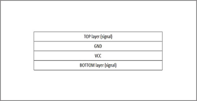
The next step is to make a multilayer board. Following the above steps to make a single panel, even if the two sides are finished, it is a double panel, but we often find ourselves with four or six (or even eight) layers of board.
To summarize, the production process of a typical pcb factory is as follows: blanking → inner fabrication → pressing → drilling → copper plating → outer fabrication → soldering paint printing → text printing → surface treatment → contour processing.
Should PCB design remove dead copper?
2023-02-23


Достаточно загрузить файлы Gerber, BOM и проектные документы, и команда KINGFORD предоставит полное предложение в течение 24 часов.