
Контрактное производство электроники под ключ в Китае
Шэньчжэнь, район Баоань, улица Фуюн, улица Фуцяо, район 3, промышленный парк Лонгхуй 6

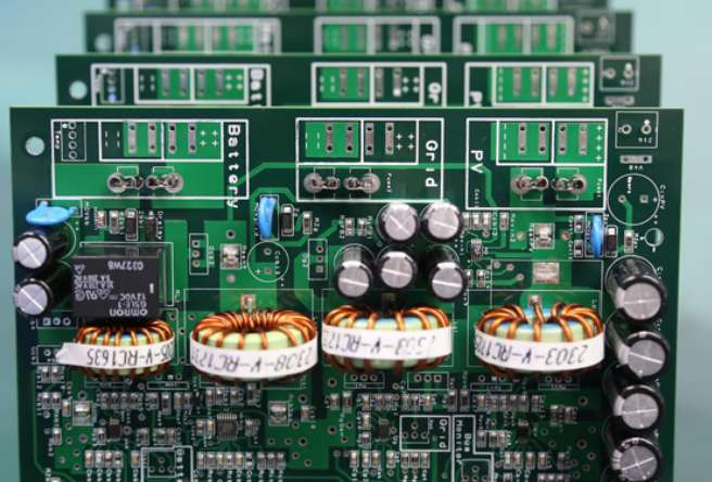
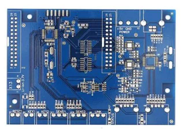
PCB design is both science and art. There are a lot of technical specifications about wiring widths, wiring layering, schematics, etc., but it gets interesting when you get to the artistic component layout in PCB design.
The fact that there are few restrictions on the placement of components and no "infallible" specifications makes the novice electronics engineer eager for personal ambition and creativity when it comes to arranging the components on the circuit board. It's entirely up to you and your design ideas.But that doesn't mean you can do whatever you want. Design in computers eventually needs to come down to earth and become something usable, so the following 10 tips for PCB placement can guide beginners through the initial stages of electronic design smoothly.
Why is component placement important?
It is true that PCB design is 90% device layout and 10% wiring. Starting with careful placement of devices can achieve twice the result with half the effort, and can also improve the electrical characteristics of PCB. What happens if you just throw the components around on the circuit board?
Waste of time: There is a good chance that you will find somewhere in the wiring process that there is not enough room to run, or that the entire wiring needs to be torn down and redone.
Circuit board doesn't work: You would think that if you put the device in place and put all the leads in place, everything would be fine. Send the design documents to the board manufacturer and wait a few days for a new board to arrive. Just as we were about to happily weld circuits, we were slapped in the face with the reality that some of the components were not weldable (either in the wrong package or in conflict with each other).
Aesthetics are broken: we have to admit that even humble electronics engineers agree with symmetry and detail in the pursuit of aesthetics. The kind of people who are lack of love and do not go at the beginning of the components of the circuit board, in the later welding and debugging process will give people feel more blockage, pouring into the eye only Ge you paralysis.
If you meet a barker, they will argue with you about where the components go and what the rules are, 100 electronics engineers will have 1,000 wiring plans for the same circuit diagram. That's why designing circuit boards is more of an artistic process.
If you're always trying to figure out what's right and wrong, here's a tip to help you figure out if your circuit board components are in the right place. After the components are laid out, use automatic wiring in board design software (such as Autodesk EAGLE). If the final failure rate is less than 85%, you need to spend more time optimizing the component placement.
Tip 1: Understand the physical limits of the board
Before placing components, you need to know exactly where the board's mounting holes, edge connectors and mechanical size limits lie.
Because these factors affect the size and shape of your circuit board. I have seen a design of a circuit board that could not fit into the circuit board fixed area, had to be redesigned.
To avoid being silly, deliberately set a clear zone for mechanical constraints (mounting holes, circuit Outlines) so you can work within the boundaries of what's allowed.
Tip 2: Make clear the circuit board manufacturing process
Also, before placing a circuit component, it's a good idea to find out a few key things from the circuit manufacturer:
1. Assembly process and test process of circuit;
2. Whether space needs to be reserved for PCB V-slot cutting;
3. Component welding process: wave soldering, zone welding or manual welding?
circuit board manufacturing process will affect the size of the gap between components. Also, if your board is going to be welded in the pipeline, you will need to leave extra space (greater than 20mil) at the edge of the board for the board to be attached to the conveyor belt. An additional fastening plate on a circuit board that is removed after the circuit board has been welded.
Tip 3: Give the integrated chip breathing room
Note that the "gasp" in question is not air, as you'll see below.
When laying out any component, you need to leave at least 350mil of space between them as much as possible, and more space for chips with lots of pins.
The more pins there are now, the denser they are. If integrated chips are too close together, there is a good chance that their leads cannot be easily routed. Often is the more difficult to wire, sometimes bother cloth through a line will consume your 100 hair, even to call every day should not, call the ground is not working dilemma. (If you had known this, why had you)
Tip 4: The same device goes in the same direction
Line them up as much as possible and keep them in a consistent formation for the same devices.
This is mainly for the convenience of the later assembly, inspection and testing of the circuit board, especially for the surface packaged devices in the wave soldering process, the circuit board uniform through the melt solder peak. Uniform placement of the device heating process uniform, can ensure high consistency of solder joint.
Tip 5: Reduce lead crossing
Reduce lead crossing by adjusting device position and direction.
Now many PCB board design software will provide a function to show that there is no connection between pin pairs. By changing the position and direction of the device to minimize lead crossing between devices, a lot of effort can be saved for later wiring.
Tip 6: Place the circuit edge first
For devices that cannot be moved arbitrarily due to mechanical constraints, such as external connectors on the circuit board, switches, USB ports, etc., should be placed first.
These devices are often located as part of the overall mechanical design of the system and cannot be changed. After placing these components, it gives you an honorable starting point for the subsequent component arrangement. Get the edge of the board down, and all that's left is the highlight of your imagination and creativity.
Tip 7: Avoid device collisions
Absolutely avoid overlapping the pads of the device or making the edges of the device overlap for wiring in Small circuit boards. It is best to maintain a distance of 40mil (1mm) between all devices.
The most important reason is to avoid short circuit failure between pads in the process of circuit manufacture. Don't forget that tight placement also makes wiring more difficult.
Also, avoid overcrowding when placing holes. The holes may also expose the copper in the future, causing a short circuit.
Tip 8: Try to put the devices on the same side
If you're designing a two-layer circuit board, the most common recommendation is to place the components on the same side.
If the device is not placed on the same side of the circuit board, it will make the later production of the circuit board laborious. The following will tell you the reason. Normally, the components on the circuit board are completed by the automatic component placement machine. The components are only on one side, and the PCB production process only needs to be repeated. Otherwise, two device placements are required. Wasting productive time is a waste of money and lives.
Tip 9: Keep chip pins and devices of the same polarity
Each integrated chip has a sign indicating the starting position of pin 1. For the orientation of the chip pin 1, or polar devices (motor capacitor, diode, transistor, LED, etc.) to maintain the same direction, will also bring convenience to the circuit board production.
If you've ever welded or tuned a circuit board yourself, you won't doubt it. Think about it. When you weld the polarity and orientation of the components on a circuit board, do you have no idea how successful you can weld the circuit board?
Tip 10: Device position is similar to schematic diagram
When placing components, mentally place them according to the position relationships on your schematic diagram.
In fact, you have optimized the positions of the components when designing the schematic (minimal wiring, minimal intersections), so stick to the positions of the components on the schematic until the PCB placement makes natural sense. In particular, in the late manual wiring, the schematic in mind will also secretly help you choose a reasonable short path to the wiring.
Creation under constraint
The best PCB design stems from the extraordinary layout of the device. Don't fool around. You should always focus on the proper placement of the components. This process is worth all the effort. It is probably the most rewarding process in PCB design. When you see the design PCB into the finished circuit board , it will be a happy time to taste the fruits of labor.
printed circuit board wiring
2023-02-16


Достаточно загрузить файлы Gerber, BOM и проектные документы, и команда KINGFORD предоставит полное предложение в течение 24 часов.