
Контрактное производство электроники под ключ в Китае
Шэньчжэнь, район Баоань, улица Фуюн, улица Фуцяо, район 3, промышленный парк Лонгхуй 6

At the beginning of a new design, because most of the time is spent on circuit board design and component selection, the PCB layout and wiring stage is often due to lack of experience, not thoughtful enough.
Failure to provide sufficient time and effort for the PCB layout and wiring phase of the design can lead to problems in the manufacturing phase or functional deficiencies as the design moves from the digital domain to the physical reality.
So what is the key to designing a circuit board that is realistic on paper and in physical form? Let's explore the first six PCB design guidelines you need to know when designing a manufacturable, functional PCB.
Fine-tune your component layout
The component placement phase of the PCB layout process is both a science and an art, requiring strategic consideration of the major components available on the board. While the process can be challenging, the way you place your electronic components will determine how easy your board is to make and how well it meets your original design requirements.
While there is a general general sequence for component placement, such as sequential placement of connectors, PCB mounting devices, power circuits, precision circuits, critical circuits, etc., there are some specific guidelines to keep in mind, including:
Orientation: Ensuring that similar components are positioned in the same direction will help achieve an efficient and error-free welding process.
Layout: Avoid placing smaller components behind larger components, which may cause mounting problems due to welding of larger components.
Organization: It is recommended to place all surface mount (SMT) components on the same side of the board and all through-hole (TH) components on top of the board to minimize assembly steps.
One final PCB design guideline to note: When using mixed technology components (through hole and surface mount components), the manufacturer may require additional processes to assemble the board, which will increase your overall cost.
Good chip component orientation (left) and bad chip component orientation (right)
Good component arrangement (left) and bad component arrangement (right)
Proper placement of power supply, grounding and signal wiring
After placing the component, you can next place power, ground, and signal wiring to ensure a clean trouble-free path for your signal. At this stage of the layout process, keep the following guidelines in mind:
(1) Locate the power supply and grounding plane
It is always recommended that the power supply and ground plane layers be placed inside the board while remaining symmetrical and centered. This helps prevent your circuit board from bending, which is also related to whether your components are positioned correctly.
For supplying power to the IC, it is recommended to use a common channel for each power channel, ensure a strong and stable cable width, and avoid Daisy chain power connections from component to component.
(2) Signal cable connection
Next, connect the signal wires as designed in the schematic diagram. It is recommended to always take the shortest possible path and direct path between components.
If your component needs to be fixed horizontally without deviation, it is recommended to route the circuit board basically horizontally where the component exits, and then vertically after the exit.
This keeps the element in place horizontally as the solder moves through the weld. As shown in the top half of the figure below. The signal routing mode in the lower part of the figure below may cause component deflection with the flow of solder during welding.
Recommended wiring (arrow indicates solder flow direction)
Unrecommended wiring (arrow indicates solder flow direction)
(3) Define the network width
Your design may require different networks that will carry a variety of currents, which will determine the desired network width. Given this basic requirement, a 0.010 "(10mil) width is proposed for low current analog and digital signals. When your line current exceeds 0.3 amps, it should be widened. There is a free line width calculator to make this conversion process easy.
Effective isolation
You may have experienced how large voltage and current spikes in the power supply circuit can interfere with your low-voltage current control circuit. To minimize such interference problems, please follow the following guidelines:
Isolation: Ensure that each power channel is kept separate from the power and control areas. If you must connect them together in the PCB board, make sure it is as close to the end of the power path as possible.
Layout: If you have placed a ground plane in the middle layer, be sure to place a small impedance path to reduce the risk of interference from any power circuits and to help protect your control signals. You can follow the same guidelines to keep your digital and analog separate.
Coupling: To reduce capacitive coupling due to placing large ground planes and running lines above and below them, try to cross analog ground only through analog signal lines.
Sample component isolation (digital and analog)
Solve the heat problem
Have you ever experienced circuit performance degradation or circuit board damage due to heat problems? As a result of not considering the heat dissipation, there have been many problems plaguing many designers. Here are some guidelines to keep in mind to help solve heat dissipation problems:
(1) Identify troublesome components
The first step is to start thinking about which components dissipate the most heat from the board. This can be done by first finding the "thermal resistance" rating in the element's data sheet and then following the recommended guidelines to transfer the heat generated. Of course, radiators and cooling fans can be added to keep components cool, and remember to keep key components away from any high heat sources.
(2) Add hot air welding pad
The addition of hot-air pads is useful for manufacturing fabricable circuit boards, and they are critical for applications of wave soldering on high copper content components and multilayer circuit boards. Because of the difficulty in maintaining process temperature, it is always recommended to use hot-air pads on through-hole elements to make the welding process as simple as possible by slowing down the rate of heat loss at the element pins.
As a general rule, always use hot air pad connections for any through or through holes connected to the ground plane or power plane. In addition to the hot air pad, you can also add teardrops where the pad connects the wires to provide additional copper foil/metal support. This will help reduce mechanical and thermal stress.
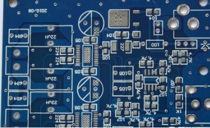
Typical hot air pad connection
Hot air welding disc science
Many engineers who are responsible for Process or SMT technology in the factory will often come across solder empty, de-solder or cold solder of the circuit board components and other non-solder problems. No matter how to change the process conditions or how to adjust the furnace temperature of reflow welding, there is a certain proportion of tin can not be welded. What the hell is going on here?
Apart from the oxidation of components and circuit boards, it is found that a large part of such poor welding actually comes from the lack of layout design of circuit boards, and the most common is that a few welding feet of components are connected to a large area of copper, resulting in poor welding of these components after reflow welding. Some hand welded components may also cause false welding or cladding problems due to similar conditions, and some may even weld the components due to excessive heating.
In general PCB design often need to lay a large area of copper foil for power (Vcc, Vdd or Vss) and Ground (GND, Ground). These large areas of copper foil will generally be directly connected to some control circuit (IC) and electronic components of the pin.
Unfortunately, if we want to heat these large areas of copper foil to the temperature of tin melting, it usually takes more time than the independent pad (that is, the heating will be slower), and the heat dissipation is faster. When one end of such a large area of copper foil wiring is connected to small components such as small resistance and capacitance, and the other end is not, it is easy to melt tin and solidification time is inconsistent and welding problems occur; If the temperature curve of reflow welding is not adjusted well and the preheating time is not enough, the welding feet of these components connected in large copper foil are easy to cause the problem of false welding because they cannot reach the tin melting temperature.
When manual welding (Hand Soldering), the welding feet of these components connected to a large piece of copper foil will be too fast because of heat dissipation, and can not be completed in the specified time. The most common adverse phenomenon is cladding welding, virtual welding, solder only welding on the component of the welding foot and not connected to the circuit board of the pad. From the appearance, the entire solder joint will form a ball; What is more, in order to weld the welding feet on the circuit board and constantly adjust the temperature of the iron, or heating for too long, so that the components exceed the heat resistant temperature and damage without knowing it.


Достаточно загрузить файлы Gerber, BOM и проектные документы, и команда KINGFORD предоставит полное предложение в течение 24 часов.