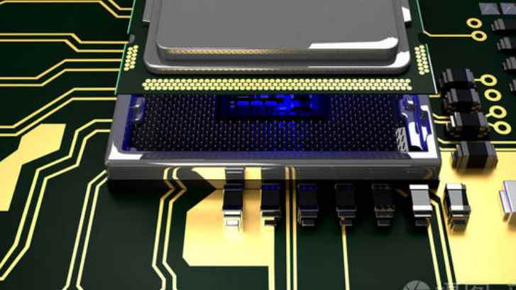
Detail PCB board ESD
One end of the triangle is connected to a signal wire and the other is connected to ground. When static electricity is present, a tip discharge is generated which consumes electrical energy.


One end of the triangle is connected to a signal wire and the other is connected to ground. When static electricity is present, a tip discharge is generated which consumes electrical energy.
5G phones will also bring new opportunities to the printed circuit board market, as Chinese mobile phone giants ZTE and Huawei announced in August that the first 5G phones will be officially sold.
For the analog part of a mixed-signal PCB and the local CPU core with 2V operating voltage, the "layout before wiring" method is not recommended. For OC48 cards, the part of the DSP analog circuit that contains the analog reference voltage and t...
The board on which the components are installed is bent after welding, and it is difficult to cut the feet of the components neatly. The board can not be installed into the chassis or machine socket, so the assembly plant encountered the board is also ver

Thinner circuit materials are commonly used in millimeter wave applications because the higher the frequency, the shorter the wave length and the smaller the circuit size.
The copper roots narrow the line spacing, resulting in the printed board does not meet the requirements of Party A, and may even be rejected. Because the rejection will make the production cost of PCB greatly increased.

The more links there are, the more likely there will be problems. This can be regarded as a very special aspect of the printed circuit production process.

Avoid running digital clock lines and high frequency analog signal lines near the power layer; otherwise, the noise from the power signal will be coupled to the sensitive analog signal.

The PCB of digital circuit can be composed of a wide ground wire circuit, that is, to form a ground network to use (the ground of analog circuit can not be used in this way) with a large area of copper layer as ground, in the printed board is not used to
There is no through hole between the welding pads of components without external pins (such as chip resistance, capacitor, adjustable potentiometer, adjustable capacitor,
Need to have a detailed understanding of PCB substrate quality (such as size and temperature stability), materials, mimeographing process capacity and relative suppliers, need to sort out and establish their own substrate specifications.

General simulation software cannot take into account some impedance discontinuity wiring conditions due to the line model or the mathematical algorithm used. In this case, only some Temninators, such as series resistors, can be reserved on the schematic d


