
Контрактное производство электроники под ключ в Китае
Шэньчжэнь, район Баоань, улица Фуюн, улица Фуцяо, район 3, промышленный парк Лонгхуй 6

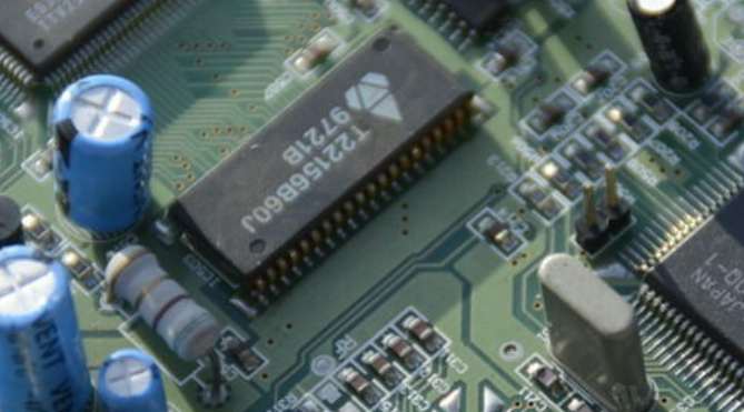
The high speed analog signal between the optical transceiver and the DSP is very sensitive to external noise. Similarly, all the special power and reference voltage circuits also create a lot of coupling between the card's analog and digital power transmission circuits. Sometimes, due to the limitations of the housing shape, high-density board cards have to be designed. Due to the orientation of the external optical cable access card and the high size of some components of the transceiver, the position of the transceiver in the card is fixed to a large extent. The system I/O connector position and signal allocation are also fixed. This is the groundwork that must be done before the layout.
As with most successful high-density analog layout and wiring schemes, the layout needs to meet the wiring requirements, and the layout and wiring requirements must be mutually compatible. For the analog part of a mixed-signal PCB and the local CPU core with 2V operating voltage, the "layout before wiring" method is not recommended. For OC48 cards, the part of the DSP analog circuit that contains the analog reference voltage and the analog power supply bypass capacitor should be wired interactively first. After the wiring is completed, the entire DSP with analog components and wiring should be placed close enough to the optical transceiver to fully ensure the shortest wiring length, minimum bending and minimum holes for high-speed analog differential signals to the DSP. The symmetry of the differential layout and wiring will reduce the effect of common-mode noise. However, it is difficult to predict the best layout before wiring.
Consult your chip distributor for PCB board design guidelines. Fully communicate with the distributor's application engineer before designing according to the guidelines. Many chip distributors have strict time limits for providing high-quality cloth recommendations. Sometimes, the solution they provide is feasible for a "Tier 1 customer" using the device. In the field of signal integrity (SI) design, the signal integrity design of new devices is particularly important. Following the distributor's basic guidelines and in conjunction with the specific requirements for each power and ground pin in the package, you can begin wiring the OC48 card with DSP and microprocessor integrated.
After the location and wiring of the high-frequency analog part is determined, the rest of the digital circuit can be placed according to the grouping method shown in the block diagram. Care should be taken to carefully design the following circuits: the location of the PLL power filter circuit in the CPU that is sensitive to analog signals; Local CPU kernel voltage regulator; A reference voltage circuit for "digital" microprocessors.
Electrical and manufacturing specifications for digital wiring can then be properly applied to the design. The aforementioned design of signal integrity for high-speed digital buses and clock signals reveals some special wiring topology requirements for processor buses, balanced Ts, and time-delay matching for some clock signal wiring. But what you may not know is that someone else has proposed an update, which is to add several terminal resistors.
In the process of solving the problem, it is natural to make some adjustments in the layout stage. However, before you begin wiring, it is important to verify the timing of the digital sections against the layout scheme. At this point, a full DFM/DFT layout review of the board will help ensure that the card meets the customer's needs.

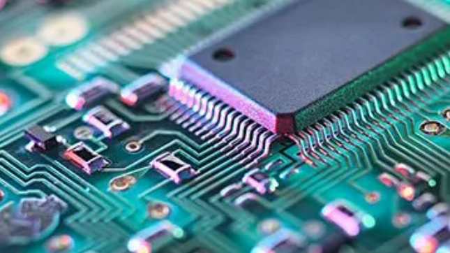
For the power lines of digital devices and the digital parts of mixed-signal DSPS, the digital wiring starts with SMD escape patterns. The shortest and widest printed line permitted by the assembly process shall be used. For high frequency devices, the printed line of the power supply is equivalent to a small inductance, which will worsen the power supply noise and cause undesired coupling between the analog and digital circuits. The longer the power supply print line, the greater the inductance.
The optimal layout and wiring scheme can be obtained by using digital bypass capacitor. In short, the position of the bypass capacitor is fine-tuned as needed to make it easy to install and distribute around the digital parts of digital components and mixed-signal devices. The same "shortest and widest route" method is used to route the bypass capacitance outlet diagram.
When the power branch is to cross a continuous plane (such as the 3.3V power layer on the OC48 interface card), the power pins and the bypass capacitor themselves do not have to share the same exit diagram to get the lowest inductance and ESR bypass. On mixed-signal PCBS such as the OC48 interface card, special attention should be paid to the wiring of the power branch. Remember to place additional bypass capacitors in a matrix arrangement throughout the card, even in the vicinity of the passive device to place the power outlet diagram to determine when automatic wiring can begin. The ATE test contacts on the OC48 card should be defined at logic design time. Make sure the ATE touches 100% of the nodes. In order to achieve an ATE test with a minimum ATE probe of 0.070 in., the breakout via locations must be preserved to ensure that the power layer is not cut off by crossing antipads on the opposite side of the breakout via.
If a power and ground opening (split) scheme is to be used, layer bias should be selected on adjacent wiring layers parallel to the opening. A no-wiring zone is defined on the adjacent layer according to the perimeter of the opening zone to prevent wiring from entering. If wiring must pass through an open area to another layer, ensure that the other layer adjacent to the wiring is a continuous grounding layer. This will reduce the reflection path. Having the bypass capacitor cross the open power layer is good for some digital signal distribution, but bridging between the digital and analog power layers is not recommended because noise is coupled to each other through the bypass capacitor.
Several new automated routing applications are capable of routing high density multilayer digital circuits. The initial wiring phase uses a large 0.050 inch hole spacing in the SMD outlet and takes into account the type of package used. The subsequent wiring phase allows the holes to be positioned close to each other so that all tools achieve the highest spread rate and the lowest number of holes. Because the OC48 processor bus uses an improved star topology, it has the highest priority when routing automatically.
summarize
After the completion of OC48 cable board, the signal integrity check and timing simulation should be carried out. Simulation results show that the wiring instruction meets the expected requirements and improves the timing index of the second layer bus. The final design rule check, final manufacturing review, light mask and review and issued to the manufacturer, then the board layout task is officially completed.


Достаточно загрузить файлы Gerber, BOM и проектные документы, и команда KINGFORD предоставит полное предложение в течение 24 часов.