
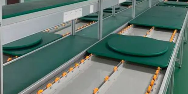
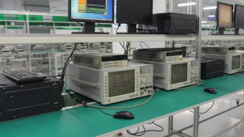
Контрактное производство электроники под ключ в Китае
Шэньчжэнь, район Баоань, улица Фуюн, улица Фуцяо, район 3, промышленный парк Лонгхуй 6

High frequency circuit design is a very complex design process, its wiring is very important to the whole design! Next, I will share some high frequency PCB design wiring skills.
High frequency PCB wiring skills
1. Multi-layer wiring
High frequency circuit often has high integration, high wiring density, using multilayer board is not only necessary for wiring, but also an effective means to reduce interference. In the stage of PCB Layout, reasonable selection of a certain number of layers of printed board size, can make full use of the intermediate layer to set shielding, better realize the nearby grounding, and effectively reduce the parasitic inductance and shorten the transmission length of the signal, but also greatly reduce the signal cross interference, all these methods are beneficial to the reliability of high frequency circuit.
2. The shorter the lead, the better
The radiation intensity of the signal is proportional to the length of the signal line. The longer the high-frequency signal lead, the easier it is to be coupled to the components close to it. Therefore, for high frequency signal lines such as signal clock, crystal oscillator, DDR data, LVDS wire, USB cable, HDMI cable, etc., the shorter the cable is required as far as possible.
3. The less bent the lead, the better

It is best to use the lead of high frequency circuit wiring fully straight line, need to turn, can be used 45 degrees fold line or arc turn, this requirement in low frequency circuit is only used to improve the copper foil fixation strength, and in high frequency circuit, meet this requirement can reduce the high-frequency signal external emission and mutual coupling.
4. The less alternations between lead layers, the better
The phrase "the less interlayer alternations of leads, the better" means that the fewer holes (Via) used in the connection of components are the better. It has been measured that a single pass hole brings about 0.5pF of distributed capacitance, and reducing the number of pass holes significantly increases speed and reduces the possibility of data errors.
5. Pay attention to crosstalk caused by short distance parallel routing of signal cables.
High frequency circuit wiring should pay attention to "crosstalk" caused by short distance parallel routing of signal lines. Crosstalk refers to the coupling phenomenon between signal lines that are not directly connected. Since high-frequency signals are transmitted along the transmission line in the form of electromagnetic waves, signal lines will play the role of antennas, and the energy of electromagnetic fields will be transmitted around the transmission line. The unwanted noise signals generated between signals due to the mutual coupling of electromagnetic fields are called Crosstalk.
The parameters of PCB board layer, the distance between signal wires, the electrical characteristics of the driver and receiver end, and the connection mode of signal wires all have a certain influence on the crosstalk.
6. The power pin of the integrated circuit block increases the high frequency decoupling capacitance
Each integrated circuit block power pin to add a high frequency dropout capacitor. Increasing the high frequency decoupling capacitance of the power supply pin can effectively restrain the interference of high frequency harmonics on the power supply pin.
7. High frequency digital signal ground wire and analog signal ground wire to do isolation
When analog ground wire and digital ground wire are connected to the public ground wire, high frequency choke magnetic beads should be used to connect or directly isolate and select the appropriate ground single point interconnection. The ground potential of high frequency digital signal ground is generally inconsistent, and there is a certain voltage difference directly between them. Moreover, the ground wire of high frequency digital signal often has a very rich harmonic component of high frequency signal. When the digital signal ground wire and analog signal ground wire are directly connected, the harmonic of high frequency signal will interfere with the analog signal through the ground wire coupling way. Therefore, under normal circumstances, the ground wire of the high frequency digital signal and the ground wire of the analog signal should be isolated, which can be used in the way of single point interconnection at the appropriate position, or the way of high frequency choke magnetic bead interconnection.
8. Avoid a loop caused by cable routing
All kinds of high-frequency signals should not form a loop. If it cannot be avoided, the loop area should be as small as possible.
9. Good signal impedance matching must be ensured
In the process of signal transmission, when the impedance is not matched, the signal will be reflected in the transmission channel, and the reflection will make the synthesized signal form overimpulse, resulting in signal fluctuation near the logical threshold.
The fundamental way to eliminate the reflection is to make the impedance of the transmission signal good match, because the load impedance and the transmission line characteristic impedance difference is larger the reflection is larger, so it should be as far as possible to make the signal transmission line characteristic impedance and load impedance equal. At the same time, it should be noted that the transmission line on the PCB should not have mutations or corners, and the impedance of each point of the transmission line should be kept continuous as far as possible, otherwise there will be reflections between the sections of the transmission line.
10. Maintain the integrity of signal transmission
Maintain the integrity of signal transmission and prevent the "ground projectile phenomenon" caused by the division of ground wire.


Достаточно загрузить файлы Gerber, BOM и проектные документы, и команда KINGFORD предоставит полное предложение в течение 24 часов.