
Контрактное производство электроники под ключ в Китае
Шэньчжэнь, район Баоань, улица Фуюн, улица Фуцяо, район 3, промышленный парк Лонгхуй 6

Shenzhen kingford is a PCBA processing manufacturer with its own SMT plant, providing one-stop PCBA processing services from electronic component procurement to PCB production and processing, SMT patches, DIP plug-ins, PCBA testing and finished product assembly
Data should be provided for PCBA patch processing
1. Complete PCB board files (Gerber files, placement maps, steel mesh files) and board making requirements;
2. Complete BOM (including model, brand, package, description, etc.);
3. PCBA assembly drawing.
PS: Report the PCBA function test fee, and provide the PCBA function test method.
PCBA patch processing process
1. Make smt production process documents and generate SMT coordinate documents according to customer Gerber documents and BOM documents;
2. Check whether all production materials are ready, make a complete set of orders, and confirm the PMC plan of production;
3. Perform SMT programming, and make the first plate for verification to ensure correct;
4. According to SMT process, make laser steel mesh;
5. Carry out solder paste printing to ensure that the solder paste after printing is uniform, good thickness and consistent;
6. Mount components on the circuit board through SMT mounter, and carry out online AOI automatic optical detection if necessary;
7. Set the perfect reflow furnace temperature curve, so that the circuit board flows through reflow welding, tin paste from paste, liquid to solid state transformation, after cooling can achieve good welding;
8. After necessary IPQC inspection;
9. DIP plug-in process will pass the plug-in material through the circuit board, and then through wave soldering for welding;
10. Necessary post-furnace process, such as cutting feet, post-welding, plate cleaning, etc.;
11. QA conducts comprehensive inspection to ensure the quality is OK.

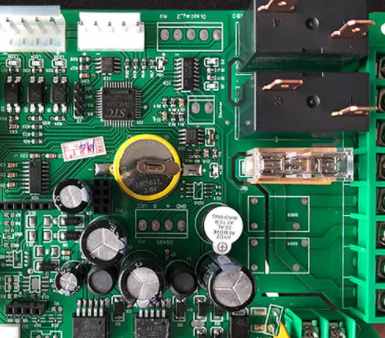
2. Types of pad in PCB design
In PCB design, pad is a very important concept, PCB engineers must be familiar with it. However, although familiar, many engineers on the pad knowledge is only a little.
What is a pad?
Pad, the basic component unit of surface mount assembly, used to form the land pattern of the circuit board, that is, a variety of pad combinations designed for special component types. A partial conductive pattern used for electrical connection, device fixation, or both.
Types of pad in PCB design
First, common welding pad
1, square pad - printed board components large but few, and printed wire is simple when more. The pad is easy to realize when making PCB by hand.
2. Circular pad -- widely used in single and double-sided printed boards with regular arrangement of components. If the density of the plate allows, the pad can be larger, welding will not fall off.
3. Island pad -- the connection between the pad and the pad is integrated. It is often used in vertical irregular arrangement installation.
4, polygon pad - used to distinguish the outside diameter close to the aperture of different pads, easy to process and assembly.
5, oval pad - This pad has enough area to enhance stripping resistance, often used in dual in-line devices.
6, open shape pad - in order to ensure that after wave soldering, so that manual repair welding pad hole is not sealed by solder often used.
Two, special pad
1, plum welding pad
Plum pad is usually used in the position of large through-hole grounding, which is designed for the following reasons:
1) The fixed hole needs to be metallized and GND connected. If the fixed hole is fully metallized, it is easy to block the hole during reflow welding.
2) The use of internal metal screw holes may be due to installation or multiple disassembly, resulting in the ground in a bad state. The use of plum hole pad, no matter how the stress changes, can ensure good grounding.
2, cross welding pad
Cross welding pad is also called hot welding pad, hot air welding pad, etc. Its function is to reduce the external heat dissipation of the pad during welding, in order to prevent virtual welding or PCB peeling caused by excessive heat dissipation.
1) When your pad is ground. Cross flowers can reduce the area of ground wire connection, slow down the heat dissipation speed, convenient welding.
2) When your PCB is a machine patch and is a reflow welder, cross stitch pads will prevent peeling of the PCB (because more heat is needed to melt the solder paste).
3. Tear drop pad
It is often used when the welding pad is connected with a thin wire, to prevent the welding pad from peeling, the wire and the welding pad from being disconnected. This pad is commonly used in high frequency circuits.
Why kingford?
1. Strength guarantee
▪SMT workshop: We have imported SMT machines and several sets of optical inspection equipment, with a daily output of 4 million. Each process is equipped with QC personnel, who can keep an eye on product quality.
▪DIP production line: We have two wave-soldering machines, among which there are more than 10 old employees who have worked for more than three years. The skilled workers can weld all kinds of plug-in materials.
2. Quality assurance, cost-effective
▪ High-end equipment can stick precision shaped parts, BGA, QFN, 0201 materials. Can also template patch, loose material hand.
▪ Sample and size batch can be produced, proofing from 800 yuan, batch 0.008 yuan/point, no start-up fee.
3. Rich experience in SMT and welding of electronic products, stable delivery
▪ Accumulated SMT SMT processing services for thousands of electronic enterprises, involving many kinds of automotive equipment and industrial control motherboard. The products are often exported to Europe and the United States, and the quality can be affirmed by new and old customers.
▪ On time delivery, normal 3-5 days after complete materials, small batch can also be expedited on the same day shipment.
4. Strong maintenance ability and perfect after-sales service
▪ Experienced maintenance engineers can repair all kinds of patch welding caused by bad products, to ensure the connection rate of each piece of circuit board.
▪ 24-hour customer service staff at any time response, the fastest speed to solve your order problems.


Достаточно загрузить файлы Gerber, BOM и проектные документы, и команда KINGFORD предоставит полное предложение в течение 24 часов.