
Контрактное производство электроники под ключ в Китае
Шэньчжэнь, район Баоань, улица Фуюн, улица Фуцяо, район 3, промышленный парк Лонгхуй 6

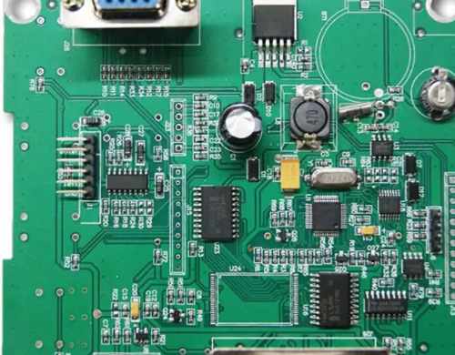
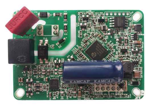
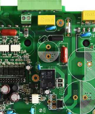
In the electronic manufacturing and processing industry, in addition to the task of researching and developing sample patches, there will also be the situation of SMT quick proofing expedited. When encountering the urgent smt quick proofing work, it is necessary not only to ensure the completion of the task within the specified time, but also to ensure the quality. Next, Shenzhen SMT manufacturer kingford will introduce how to improve the speed of SMT patch proofing and what preparatory work needs to be done.
How to improve the speed of SMT patch proofing while ensuring the quality
First, whether it is an urgent task or not, it is good to know how to improve the speed of SMT patch proofing, which can also improve the working efficiency of SMT patch processing at ordinary times. When encountering tasks requiring rapid processing, SMT patch processing data should be prepared in advance, such as patch bom, position coordinates, patch drawings and samples, so as to prepare the off-line procedures of patches in advance.
Secondly, the SMD materials must be exquisite, not all SMT patches are ready for proofing. There are still problems in the SMD materials, from the quantity of incoming materials to the specific specifications and parameters of the materials, we must pay attention to, so that there will be no problems in the processing of SMD materials.
Third, SMT SMT sample making workshop works in two shifts, so the information to be marked on bom must be marked, otherwise there is no way to ask if there is any problem in the night shift. For the original parts of incoming resistance, it is necessary to mark whether the accuracy is 1% or 5%; for incoming capacitor, it is necessary to explain the voltage number of components, and whether IC chip audion can be used instead. All these should be noted on the bom. Otherwise, the processing speed will be affected when verifying these information during SMT patch processing. Therefore, the preparatory work before processing cannot be ignored.
To improve the speed of SMT rapid proofing naturally not only reflected in the preparation before processing just mentioned, in the SMT patch processing as a technician to ensure the best state to reduce the error rate, so as to ensure the quality and quantity of SMT patch processing speed.

SMT patch processing capability
1. Maximum board card: 310mm*410mm(SMT);
2. Maximum plate thickness: 3mm;
3. Minimum plate thickness: 0.5mm;
4. Minimum Chip parts: 0201 package or parts above 0.6mm*0.3mm;
5. Maximum weight of mounted parts: 150g;
6. Maximum parts height: 25mm;
7. Maximum parts size: 150mm*150mm;
8. Minimum spacing of pin parts: 0.3mm;
9. Minimum ball parts (BGA) spacing: 0.3mm;
10. Minimum ball parts (BGA) ball diameter: 0.3mm;
11. Maximum parts mounting accuracy (100QFP) : 25um@IPC;
12. Patch capacity: 3-4 million points/day.
2. Where can I do the PCB wiring design?
kingford can provide multi-layer, high density, high speed pcb routing design and PCB design proofing services.
Data should be provided for pcb routing design
1. Schematic diagram: complete electronic document format that can produce correct netlist;
2. Mechanical size: provide the specific position and direction identification of the positioning device, as well as the identification of the specific height limit position area;
3. BOM list: mainly for the purpose of determining and checking the package information specified on the schematic diagram;
4. Wiring guide: description of specific requirements for special signals, as well as design requirements of impedance, lamination, etc.
pcb routing design ability
Maximum signal design rate: 10Gbps CML differential signal;
Maximum number of PCB design layers: 40;
Minimum line width: 2.4mil;
Minimum line spacing: 2.4mil;
Minimum BGA PIN spacing: 0.4mm;
Minimum mechanical hole diameter: 6mil;
Minimum laser drilling diameter: 4mil;
Maximum number of pins:; 63000 +
Maximum number of components: 3600;
Maximum number of BGA: 48+.
pcb routing design principles
1. In accordance with the layout principle of "big before small, difficult before easy", that is, important unit circuits and core components should be laid out first.
2. Major components are arranged according to the principle diagram and the main signal flow pattern of boards.
3. The arrangement of components should be convenient for debugging and maintenance, that is, large components should not be placed around small components, and there should be enough space around the components to be debugged.
4. The same structure of the circuit, as far as possible to use "symmetrical" standard layout;
5. Optimize the layout according to the standards of uniform distribution, balanced center of gravity and beautiful layout;
6. The plug-in components of the same type shall be placed in the X or Y direction in the same direction. The same type of polar discrete components should also strive to keep consistent in the X or Y direction, easy to produce and test.
7. The heating element should be evenly distributed in general to facilitate the heat dissipation of the veneer and the whole machine. In addition to the temperature detection element, the temperature sensitive device should be far away from the components with large heat.
8. The layout should meet the following requirements as far as possible: the overall connection should be as short as possible, and the key signal line should be the shortest; High voltage and high current signals are completely separated from low current and low voltage weak signals; Analog signals are separated from digital signals; High frequency signals are separated from low frequency signals; The spacing of high-frequency components should be sufficient.
9. The layout of the decoupling capacitor should be as close to the IC power pin as possible, and the circuit formed between the power supply and the ground should be the shortest.
10, component layout, should be appropriate to consider the use of the same kind of power device together as far as possible, in order to facilitate the future power separation.
pcb routing design service flow
1. The customer provides schematic diagram to consult PCB design;
2. Evaluate quotation according to schematic diagram and customer design requirements;
3. The customer confirms the quotation, signs the contract and pays the project deposit;
4. Received advance payment and arranged engineer design;
5. After the design is completed, provide the screenshot of the document to the customer for confirmation;
6. The customer confirmed OK, settled the balance, and provided PCB design materials.
Why kingford?
1. Strength guarantee
▪SMT workshop: We have imported SMT machines and several sets of optical inspection equipment, with a daily output of 4 million. Each process is equipped with QC personnel, who can keep an eye on product quality.
▪DIP production line: We have two wave-soldering machines, among which there are more than 10 old employees who have worked for more than three years. The skilled workers can weld all kinds of plug-in materials.
2. Quality assurance, cost-effective
▪ High-end equipment can stick precision shaped parts, BGA, QFN, 0201 materials. Can also template patch, loose material hand.
▪ Sample and size batch can be produced, proofing from 800 yuan, batch 0.008 yuan/point, no start-up fee.
3. Rich experience in SMT and welding of electronic products, stable delivery
▪ Accumulated SMT SMT processing services for thousands of electronic enterprises, involving many kinds of automotive equipment and industrial control motherboard. The products are often exported to Europe and the United States, and the quality can be affirmed by new and old customers.
▪ On time delivery, normal 3-5 days after complete materials, small batch can also be expedited on the same day shipment.
4. Strong maintenance ability and perfect after-sales service
▪ Experienced maintenance engineers can repair all kinds of patch welding caused by bad products, to ensure the connection rate of each piece of circuit board.
▪ 24-hour customer service staff at any time response, the fastest speed to solve your order problems.


Достаточно загрузить файлы Gerber, BOM и проектные документы, и команда KINGFORD предоставит полное предложение в течение 24 часов.