
Контрактное производство электроники под ключ в Китае
Шэньчжэнь, район Баоань, улица Фуюн, улица Фуцяо, район 3, промышленный парк Лонгхуй 6

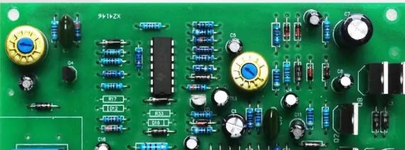
PCB board bending or warping is usually caused by one or a combination of the following causes:
1. Temperature change: Temperature change will cause thermal expansion or contraction of PCB board. If the sides of the sheet are not affected by the same heat, it will cause the sheet to bend or warp.
2. Uneven plating: Uneven plating may result in a thicker copper layer on one side of the plate and a smaller one on the other. This causes the sheet to deform.
3. PCB board uneven thickness: Uneven thickness of PCB board may cause bending or warping. This may be due to material changes during production or pressure changes in the plate.
4. Improper board size: If the PCB board size is incorrect, it may cause bending or warping of the board. This can be due to a design error or an error in the manufacturing process.
5. Uneven welding: If the components on the board are not evenly welded, it may lead to bending or warping of the board. This can be due to errors in manufacturing or problems in the assembly process.
6. Poor sheet quality: Low quality sheet may cause sheet bending or warping. This may be due to material defects or quality problems in the production process.
7. PCB board processing is improper: if the error is too large during the processing of the board, it may lead to bending or warping of the board. This may be due to errors in the machining process or machine failure.
8. PCB board material issues: PCB board materials may not be suitable for manufacturing requirements, which may cause the board to bend or warp.
9. PCB board design problems: Design problems may cause the board to bend or warp. This can be due to factors not considered by the designer or due to errors in the design process.
10. Mechanical stress: During transportation, installation or use, mechanical stress may cause bending or warping of PCB board.
To avoid bending or warping of PCB boards, the following measures should be taken:
1. Select the appropriate board thickness and size: When designing the PCB, the appropriate board thickness and size should be selected according to the actual needs to ensure that the board can withstand the expected load and will not appear excessive bending or warping.
2. Pay attention to plating uniformity: In the manufacturing process of PCB board, it should be ensured that the plating is uniform to avoid the problem of too thick copper layer on one side of the board and too thin on the other side, which will lead to bending or warping of the board.
3. Control machining errors: During the processing of PCB board, errors should be strictly controlled to ensure that the size and shape of the board meet the design requirements and avoid excessive bending or warping problems.
4. Reasonable arrangement of components: In the design and assembly process of PCB board, the location and spacing of components should be arranged reasonably to avoid uneven distribution of components on the board, which will lead to bending or warping of the board.
5. Control welding temperature and time: During the welding process of PCB board, the welding temperature and time should be controlled to avoid excessive heating or long heating time, which may lead to bending or warping of the board.
6. Pay attention to temperature changes: During the use and storage of PCB board, pay attention to temperature changes to avoid bending or warping caused by the thermal influence of different sides of the board.
7. Add support structure: During the design and assembly of PCB board, support structure can be added to enhance the stiffness of the board and avoid bending or warping of the board.
8. Add frame or frame: In the design and assembly process of PCB board, frame or frame can be added to enhance the stability and stiffness of the board, to avoid bending or warping of the board.
In short, PCB board bending or warping is caused by a combination of factors. In order to avoid such problems, it is necessary to take corresponding measures in the design, manufacturing, assembly and use of PCB board, and strictly control the quality and error of each link, to ensure the quality and stability of the board.

2. How to remove excess tin residue in SMT patch processing?
SMT patch machining is an efficient electronic manufacturing technique that allows the rapid placement of electronic components (such as chips, capacitors, resistors, etc.) onto the PCB surface. In this process, a large amount of solder paste will be used to ensure reliable connection between the components and the PCB surface. However, due to a number of reasons in the manufacturing process (such as improper operation, quality of materials, etc.), excess paste and slag can occur. Excess solder paste and tin slag will not only affect the quality and reliability of electronic components, but also cause damage to PCB surface. Therefore, the removal of excess tin slag is a very important step in SMT patch processing. Below, we will introduce some common methods of removing excess tin residue.
1. Manual cleaning method
Manual cleaning is one of the simplest and most primitive methods to remove excess tin residue. It is mainly operated by hand, using hand tools (such as scissors, scrapers, airbrush, etc.) to clean up excess tin residue. The advantage of this method is that it is simple and easy to operate. It does not require any equipment and materials. Only operators with certain skills and experience are needed. In addition, the manual cleaning method can be personalized to different PCB boards and tin slag, with high flexibility and plasticity. However, manual cleaning method also has many shortcomings, such as low efficiency, easy to make mistakes, work intensity, low accuracy. Moreover, if not thoroughly cleaned, some small tin residue and stains may be left, affecting the quality and reliability of the PCB surface.
2. Solvent cleaning method
Solvent cleaning is a commonly used method to remove excess tin residue. It mainly through chemical reactions, the use of solvents to dissolve or separate the excess tin residue. In general, commonly used solvents include acids, bases, organic solvents and so on. The advantages of this method are high cleaning efficiency, cleaning process will not cause damage to the PCB surface, suitable for all kinds of PCB board and tin slag. Moreover, solvent cleaning method can also add some surfactants or emulsifiers, in order to improve the cleaning effect and stability. However, solvent cleaning method also has some disadvantages, such as low safety, complex operation and high cost. In addition, due to the uncertainty of chemical reaction, the cleaning effect is also different.
3. Adhesive tape cleaning method
Viscous tape cleaning is a common method to automatically remove excess tin residue. It can realize the purpose of automatic cleaning by sticking the adhesive tape on the PCB surface and gluing the excess tin slag to the tape. The advantages of this method are high cleaning efficiency, high cleaning precision, suitable for all kinds of PCB board and tin slag. Moreover, the viscous coil cleaning method can realize continuous automatic cleaning, improve production efficiency and quality stability. However, adhesive tape cleaning also has some disadvantages, such as higher cost, more equipment and maintenance costs. In addition, for some small tin slag or hard-to-reach locations on the PCB surface, the adhesive tape cleaning method may not be suitable.
4. Aerosol cleaning method
Aerosol cleaning is a common method to remove excess tin residue. It is mainly by spraying a chemical cleaner on the PCB surface, and then using compressed air to wash away excess tin residue from the surface. The advantages of this method are high cleaning efficiency, high cleaning precision, suitable for all kinds of PCB board and tin slag. Moreover, the aerosol cleaning method will not cause damage to the PCB surface, and the solubility and fluidity of the cleaning agent can be effectively controlled. However, the aerosol cleaning method also has some disadvantages, such as high equipment cost, complex operation, environmental and health impacts.
5. Paint cleaning method
Paint cleaning is a relatively novel method to remove excess tin residue. It is mainly done by coating a layer of paint on the PCB surface, and then after the paint is dry, the excess tin slag is stripped away with the paint, so as to achieve the purpose of cleaning. The advantages of this method are high cleaning efficiency, high cleaning precision and less influence on PCB surface and environment. Moreover, the paint cleaning method can be customized according to different PCB boardand tin slag treatment, improve the cleaning effect and stability. However, the paint cleaning method also has some shortcomings, such as complex operation, the need for certain technology and experience, coating cost is higher.
The above are several common methods for removing excess tin slag. According to the actual situation and requirements of production, different methods can be selected for cleaning. At the same time, no matter what method is used, safety and environmental protection should be paid attention to.


Достаточно загрузить файлы Gerber, BOM и проектные документы, и команда KINGFORD предоставит полное предложение в течение 24 часов.