
Контрактное производство электроники под ключ в Китае
Шэньчжэнь, район Баоань, улица Фуюн, улица Фуцяо, район 3, промышленный парк Лонгхуй 6

What inspection should PCB light board finish before shipment? Many friends are concerned about this problem. PCB light board needs to go through multiple inspections and can be shipped only after the shipment inspection report is issued. Next, Shenzhen PCB Board factory - Shenzhen kingford will introduce the shipment inspection project of PCB light board to you.
First, basic inspection
Sheet material information: type, finished sheet thickness, outer copper foil, inner copper foil, warping degree, ink, color, position, marking, minimum line width, line distance, ring width, solder resistance, surface treatment, special process, test items, film, etc.
Ii. Electrical performance test report
1, test category: single and double side, general, special, test number.
2, test parameters: current, voltage, on-resistance, insulation voltage and so on.
Iii. Metallographic section analysis report
Copper thickness, nickel thickness, gold thickness, lead tin thickness, line copper thickness, roughness, etching factor, coating cracks, resin shrinkage, coating cavity, delamination and so on.
Four, impedance test.
PCB board making ability
Energy production from 2 layers to 14 layers, 14-22 layers can be proofing production.
Minimum line width/spacing: 3mil/3milBGA Spacing :0.20MM
Minimum aperture: 0.1mm Size :610mmX1200mm
Ink: Tamura, Taiyo, Fudoken;
FR4: Shengyi, Kingboard, Harbour, Hongren, Guoji, Hezheng, Nanya,
(Shengyi S1130/S1141/S1170),Tg130℃/ Tg170℃ T g180℃ and other high TG plates)
High frequency plate: Rogers, Taconic, ARLLON;
Surface process: tin spray, lead-free tin spray, gold plating, full plate gold plating, plug gold plating, full plate thick gold, chemical tin (silver), anti-oxidation (OSP) blue glue, carbon oil

PCB allegro, sample delivery date
Double-sided allegro can be completed in 24 hours, multi-layer allegro can be completed in 2-5 days;
Single/double-sided (0.6-1.6mm FR4) delivery time: 3-4 days;
Four-layer plate (0.6-1.6mm FR4) delivery time: 5-6 days;
Six-layer plate (0.8-1.6mm FR4) Delivery time: 7-8 days.
2. Analysis of the influence of welding resistance layer on BGA welding quality in PCBA processing
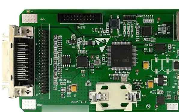
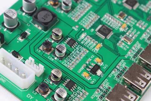
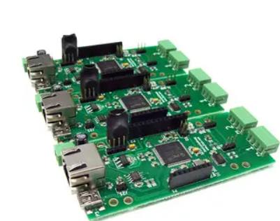
Shenzhen kingford has more than 20 years of PCBA processing experience, and has its own PCB board factory and SMT patch factory. We can provide one-stop PCBA processing services from upstream electronic components procurement to PCB board manufacturing, SMT patch, DIP plug-in, PCBA testing and finished product assembly. Next, the influence analysis of welding resistance layer on BGA welding quality in PCBA processing is introduced.
Analysis of the influence of welding resistance layer on the welding quality of BGA in PCBA processing
Solder resistance is the core of dual row QFN process design.
(1) The extension distance of welding resistance thickness on the surface of the pass-hole pad.
(2) Extension distance of solder resistance thickness of wire surface.
(3) welding resistance thickness between pads.
Case study 1:
A BGA chip launched by a company is a kind of LGA package with heat sink pad. The center distance of the welding end of the chip is 0.47mm. The welding end is ∅0.27mm round and bulged out the packaging ground. The side of the welding end is bare copper and has poor wettability. There is a large cooling pad in the middle.
Since the distance between the welding plates is relatively small, the main problem encountered in welding, especially in the SMT patch process, is bridging, so the 0.01mm thick steel mesh and ∅0.22mm window-opening design is used in production, and the bridging probability is about 1%.
Reason analysis: BGA welding with dense pins and narrow spacing is easy to produce bridging defects. The fundamental reason is caused by the structure of the package itself -- the protruding welding end, due to the unstable wetting of the side, it is easy to form a local moist weld shape on the side. Therefore, the use of relatively strong activity of the solder paste is a good way.
In addition, in PCBA process, the high and low coverage of solder paste in hot pad may be an important factor, which reduces the thickness of the weld and makes the peripheral solder joints more sensitive to the amount of solder paste. The manufacturer recommends covering about 20%. The main hope is to control the weld thickness of the heat sink pad within the range of 10 ~ 25m, in an attempt to force good wetting of the welding spot. But it is precisely this that may be the main factor in creating the bridge - reducing the amount of space the molten solder can hold. According to experience, the weld thickness of heat sink pad should be increased to more than 40um.
In addition, the inverted trapezoid welding end makes the original minimal interval further reduced; The thickness of the welding pad is also the main factor causing the bridge, which is the experience of Shenzhen patch processing plant summed up over the years.
Shenzhen kingford is a professional manufacturer of printed circuit board manufacturing, 20 years focused on single, double-sided, multi-layer circuit board production. Can provide impedance board, HDI board, blind hole plate and other multi-layer PCB board proofing, small batch production business.


Достаточно загрузить файлы Gerber, BOM и проектные документы, и команда KINGFORD предоставит полное предложение в течение 24 часов.