
Контрактное производство электроники под ключ в Китае
Шэньчжэнь, район Баоань, улица Фуюн, улица Фуцяо, район 3, промышленный парк Лонгхуй 6

Before introducing how to perform functional testing after PCBA processing, it's a good idea to understand how it was performed in the past. The best way to get a sense of actual testing is to visit a PCBA processing plant where similar products are made and view the entire production line, from the circuit board to the shop floor, all the way to product packaging and shipping. The secret of this is that we can actually experience the various processes of the product during the production process, which is very helpful for us to understand how the board is made. Next, introduce the PCBA processing function test process.
PCBA processing function test process
1. Functional test plan
Prior to SMT machining of the circuit board, there are usually DFM instructions in the design process. This will allow you to participate in the timing of "design for testability" throughout the design process. It will clearly state which aspects of the test are included in the schematic, PCB layout, and even the microcontroller code.
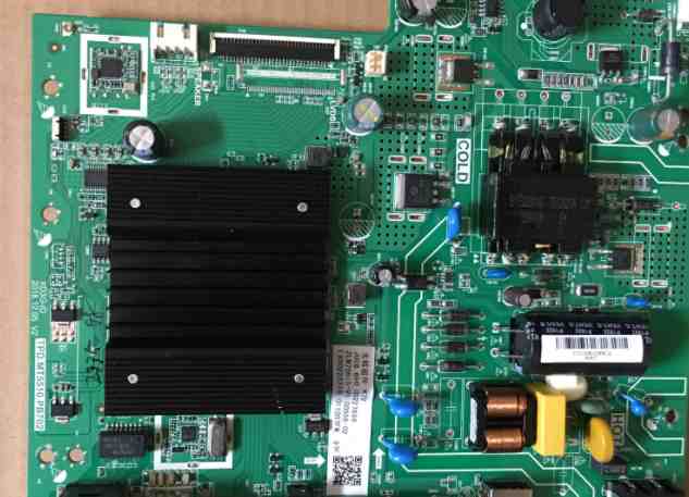
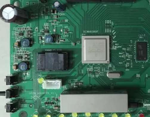
Patch processing
For example, if the user touches a capacitive touch screen, what do you want the action to do? Maybe it wakes up the screen or turns on the LED and tells the microcontroller to do something. This operation requires that all your components have the correct voltage, that capacitive touch sensors and leds are installed correctly, and that the microcontroller has been programmed and operated as intended. This functional testing program will guide the entire PCBA circuit board machining with significant quality assurance.
2. Test points
The test point is only the PCB pad on the circuit board, which is designed for easy detection. For a variety of reasons, you don't want to rely on pins or pads for probing components. The size of these pads is not specified, but should be large enough to make contact with the test probe.
3. System programming
If you look at the innards of any sufficiently sophisticated product, you will probably find either a programming connector on the PCB or an empty spot where the programming connector can be placed. This connector is commonly used to program microcontrollers already installed on PCBS and is therefore called "in-system". In a mass production scenario, it does not make sense to install this header. It is used by designers for debugging purposes rather than installed in the production process to eliminate costs.
4. Test the fixture
For early prototypes or small-scale designs, you can manually test each board yourself. You will be grateful for your future self completion of this exercise, as it enables you to appreciate and understand how to verify that your product works properly. Humans are generally not good at repetition, so having a test plan, even with checkboxes, can help you avoid skipping any steps.
In kingford, we will carry out relevant functional tests in strict accordance with customers' requirements, and complete all the pre-market inspections of customers' products.
2. Design standards for shape and size of pad
PCB design is based on the circuit schematic diagram to achieve the function required by the circuit designer. PCB design mainly refers to layout design, which needs to consider the layout of external connections, the optimal layout of internal electronic components, the optimal layout of metal wires and through holes, electromagnetic protection, heat dissipation and other factors. Excellent PCB design can save production cost, achieve good circuit performance and heat dissipation performance.
kingfor is a professional PCB design company with more than 20 years of PCB design experience. We can provide one-stop service from PCB design to PCBA OEM. Next, we will introduce the design standards of the shape and size of welding pad in PCB design.
1. Common pad shape in PCB design
Welding pad can be divided into 7 categories, according to the shape of the distinction is as follows:
1. Square pad - PCB board components are large but few, and printed wire is simple.
2. Circular pad - widely used in the regular arrangement of components of the single, double-sided PCB board.
3. Island pad - the connection between the pad and the pad is integrated, which is often used in vertical irregular arrangement installation.
4. Tear drop pad - when the connection of the line is thin often used, commonly used in high-frequency circuit.
5. Polygonal pad - used to distinguish the outside diameter close to the aperture of the pad, easy to process and assembly.
6. Oval pad - This pad has sufficient area to enhance stripping resistance and is often used for dual-in-line devices.
7. Open shape pad - In order to ensure that after wave soldering, so that manual repair welding pad hole is not blocked by solder often used.

2. Design standards for shape and size of pad in PCB design
1. The minimum single side of all pads shall be no less than 0.25mm, and the maximum diameter of the whole pad shall be no more than 3 times of the component aperture.
2. Try to ensure that the spacing between the edges of the two pads is greater than 0.4mm.
3. In the case of dense wiring, oval and oblong pad is recommended.
4. For plug-in components, in order to avoid copper foil breaking during welding, single-sided connecting disks should be completely covered with copper foil, while double-panel minimum requirements should be teardrops.
5. The organic inserted parts shall be designed as dripping pads along the elbow to ensure that the solder joints at the elbow are full.
6. The welding pad on the large area of copper skin should be chrysanthemum-shaped, without virtual welding.
The above is the introduction of the design standard of the shape and size of the welding pad in PCB design. If you have the needs of PCB design and PCBA OEM, please contact us. Next, we will introduce our PCB design capacity and PCBA processing capacity.
PCB design capability
Maximum signal design rate: 10Gbps CML differential signal;
Maximum number of PCB design layers: 40;
Minimum line width: 2.4mil;
Minimum line spacing: 2.4mil;
Minimum BGA PIN spacing: 0.4mm;
Minimum mechanical hole diameter: 6mil;
Minimum laser drilling diameter: 4mil;
Maximum number of pins:; 63000 +
Maximum number of components: 3600;
Maximum number of BGA: 48+.
PCBA processing capability
1. Maximum board card: 310mm*410mm(SMT);
2. Maximum plate thickness: 3mm;
3. Minimum plate thickness: 0.5mm;
4. Minimum Chip parts: 0201 package or parts above 0.6mm*0.3mm;
5. Maximum weight of mounted parts: 150g;
6. Maximum parts height: 25mm;
7. Maximum parts size: 150mm*150mm;
8. Minimum spacing of pin parts: 0.3mm;
9. Minimum ball parts (BGA) spacing: 0.3mm;
10. Minimum ball parts (BGA) ball diameter: 0.3mm;
11. Maximum parts mounting accuracy (100QFP) : 25um@IPC;
12. Patch capacity: 3-4 million points/day.


Достаточно загрузить файлы Gerber, BOM и проектные документы, и команда KINGFORD предоставит полное предложение в течение 24 часов.