
Контрактное производство электроники под ключ в Китае
Шэньчжэнь, район Баоань, улица Фуюн, улица Фуцяо, район 3, промышленный парк Лонгхуй 6

The introduction of SMT lead-free machining has always been a challenge for PCBA first assembly, as it will face more challenges when PCBA rework is required. Performing PCBA rework in a lead-free environment will have higher cost, quality detail, time and repeatability issues, but all of these issues need attention due to lead-free requirements.
SMT lead-free process requirements:
1. Train operators to perform lead-free assembly, maintenance and inspection, and assess time and cost.
2. Lead-free solder materials are more expensive than traditional solder, such as lead-free wire, electrode and core solder.
3. Processing temperature of lead-free assembly (about 30-35℃) requires high precision and precision.
4. Lead-free process also requires research and planning of smt processing plant to establish correct PCBA repair process.
kingford Shenzhen believes that the best practice for PCBA rework is to first train and instruct technicians and develop profiles based on the characteristics of the lead-free process. Rework criteria are defined. The process begins the same way whether standard or lead-free solder is required or not. The steps required are as follows:
1. Define and execute accurate thermal profiles
2. Delete the faulty component
3. Clean all rust or solder residue on site and prepare new parts
4. Replace parts with new solder, flux, and reflow soldering
5. Thoroughly review the rework
Accurate and reliable rework is more difficult in lead-free environments because the PCBA and the component closest to the part to be serviced must withstand multiple high-temperature cycles. In order to protect the stability of the circuit board, the preheating temperature should be set to no higher than the glass transition temperature of the PCB material.
The subsequent steps involved in the rework process depend on whether there is a lead free requirement. The difference between standard and lead-free presents a number of challenges that can only be addressed by the introduction of new or changed processes, including more rigorous and precise thermal profiles and extremely high accuracy throughout the PCBA rework process. This would avoid many costly problems caused by different heat distributions.
SMT lead-free processing
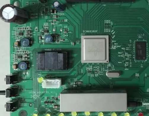
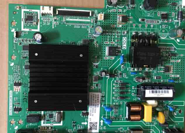
2. Difference between double panel and four layer plate in SMT processing
SMT processing is based on PCB, that is, printed circuit board, they are differentiated by the number of layers, such as double panel and four layer board. At present, it can do up to 48 layers, and from a technical point of view, the number of layers in the future is infinite. Some supercomputers have hundreds of layers, but the most common number of layers in a medical electronics PCBA or an Automotive Electronics PCBA is usually two or four. If you want to know how to choose the number of PCB layers properly, please see the following introduction on the difference between two and four layers of SMT machining before you decide!

Double panel
Dual panels are easier to use because of their simple design compared to four-ply panels. While not as simple as a single panel, they are as simple as possible without sacrificing double-sided input capabilities. The reduced complexity results in an equally reduced price tag, but that means fewer possibilities compared to four-ply panels. However, as the most commonly used circuit board in the industry, its significant advantage is that the signal has no propagation delay.
Four-ply plate
Four-ply panels have a larger surface area than two-ply panels, increasing the possibility of more wiring. As such, they are ideal for more complex devices. Because of their complexity, production costs will be higher and development slower. They are also more likely to have propagation delays or interact with each other, so proper design is very important.
So what's the use of layers?
The most important layer in the PCB is the copper foil signal layer, which is the name of the PCB. While dual panels have two signal layers, 4-layer PCBS have four. These signal layers are used to connect to other electronic components in the device. Between these layers is an insulating layer or core, which is added between the signal layers to give them structure. In the four layers, there is also a solder stop layer, which is applied on top of the signal layer. This prevents the copper trace from interfering with the other metal components on the PCB. They also have a silk-screen layer for adding numbers to different components, making them easier to lay out.
Why do you choose Shenzhen kingford for SMT lead-free processing?
1. Strength assurance
▪ SMT workshop: We have imported SMT machines and a variety of optical testing equipment, capable of producing 4 million pieces per day. Every process is equipped with QC personnel who can keep a close eye on product quality.
▪ DIP production line: There are two wave welding machines. Among them, there are more than ten old employees who have worked for more than three years. Skilled workers can weld all kinds of insert materials.
2. Quality assurance, high cost-effective
▪ High-end equipment can mount precision heterosexual parts, BGA, QFN, 0201 materials. Proofing can be machine paste, also can be hand pendulum.
▪ Samples and large and small batches can be produced. Proofing starting price 800 yuan, batch starting price 0.008 yuan/point, no start-up fee.
3. Rich experience in SMT and welding of electronic products, stable delivery time
▪ Has served thousands of home appliance subsidiaries, involving various kinds of automotive equipment and industrial control motherboard SMT SMT processing services. Products are often exported to Europe and the United States, the quality of new and old customers affirmed.
▪ On time delivery, usually within 3-5 days after the board is assembled, small batch expedited can also be shipped on the same day.
4. Strong maintenance ability and perfect after-sales service
▪ Experienced maintenance engineers are able to repair defective products caused by various welding problems and ensure the connectivity rate of each circuit board.
▪ 24-hour customer service staff will be ready to respond and resolve your order as soon as possible.


Достаточно загрузить файлы Gerber, BOM и проектные документы, и команда KINGFORD предоставит полное предложение в течение 24 часов.