
Контрактное производство электроники под ключ в Китае
Шэньчжэнь, район Баоань, улица Фуюн, улица Фуцяо, район 3, промышленный парк Лонгхуй 6

PCB design technology is very complex, involved in all aspects of many problems, to do PCB design requires the accumulation of experience, Shenzhen kingford professional PCB design for more than 20 years, next to share eight common technical problems of PCB design.
Eight common technical problems of PCB design
1, the design of a system containing DSP, PLD, from which aspects to consider ESD?
A: In terms of the general system, the main consideration of the body directly in contact with the part, on the circuit and the mechanism for appropriate protection. How much impact ESD will have on the system depends on the situation.
2. In EMC test, it is found that the harmonic of the clock signal exceeds the standard seriously. Only the decoupling capacitor is connected on the power pin. What aspects should be paid attention to in the design to suppress electromagnetic radiation?
A: The three elements of EMC are radiation source, transmission route and victim; The transmission channels are divided into space radiation transmission and cable conduction. So to suppress harmonics, first look at the way it travels. Power decoupling is the solution to conduction-mode propagation, in addition, the necessary matching and shielding is also required.
3. Why are some of the products designed with 4 layers paved and some are not?
A: The role of paving: 1, shielding; 2, heat dissipation; 3. Reinforce; 4. Technological processing needs. No matter how many layers of board paving, first of all to look at its main reason. Here we are mainly talking about high speed. Surface paving is good for EMC, but the copper paving should be as complete as possible to avoid islands.
4, frequency more than 30M plate, the use of automatic wiring or manual wiring?
Answer: Automatic or manual wiring depends on the support of software wiring function. Some wiring may be better than automatic wiring, but some wiring, such as check wiring, bus delay compensation wiring, automatic wiring effect and efficiency will be much higher than manual wiring.
5, in the design, the ground is usually divided into protective ground and signal ground; Power ground is divided into digital ground and analog ground, why to divide the ground wire?
A: The purpose of dividing the ground is mainly due to EMC concerns that the digital part of the power supply and ground noise will interfere with other signals, especially analog signals through the transmission path. No matter how divided, the final earth is only one.
6, in the cloth clock, is it necessary to add ground wire shield on both sides?
Answer: Whether to add shielding ground wire should be decided according to the crosstalk /EMI situation on the board. If the shielding ground wire is not handled well, it may make the situation worse.
7. What are the corresponding countermeasures for distributing clock lines of different frequencies?
A: For the wiring of the clock line, it is best to carry out signal integrity analysis, formulate the corresponding wiring rules, and carry out wiring according to these rules.
8, single-layer plate manual wiring, how to represent the jumper?
A: The jumper is a special device in the design, only two pads, the distance can be fixed length, can also be variable length. Manual wiring can be added as required. There will be a straight line on the board, the material sheet will also appear.
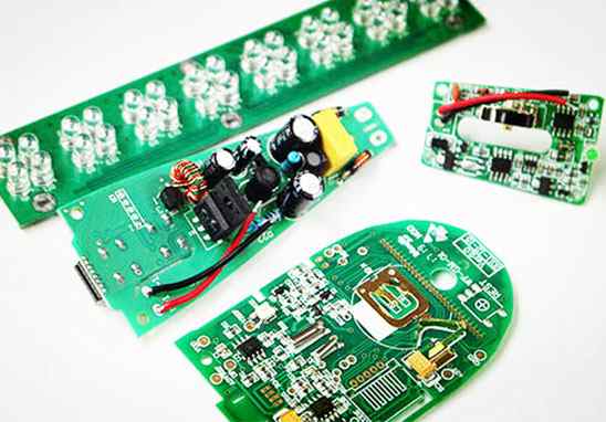
2. Charging rules and requirements for PCB circuit board proofing
A lot of novice always do not know the PCB circuit board proofing fee rules and requirements and proofing needs to provide what materials?
First, PCB circuit board proofing how to charge?
First of all, we should see what kind of board is used. The board has FR4, high TG board, brand benefit and so on. Plate is not the same, the price is not the same. In addition, look at the design drawings, the smaller the line width and line distance, the more holes, the more accurate, the higher the cost. Third, look at the surface treatment, sinking gold, gold plating than tin plating, OSP expensive. Four look at the quantity. Fifth, looking at the delivery date, the urgent cost of PCB which needs to be expedited is more expensive compared with the normal delivery date.
Two, PCB circuit board proofing need to provide what samples?
The quotation information needs to be provided to the manufacturer, and the GEBER file is generally provided for the drawings. There are clear process requirements and quantity. pcb manufacturer can follow up the quotation. After the price is decided, the manufacturer will place an order and start production.
Three, PCB circuit board proofing steps
First, determine the drawing and process, order and production process data; Secondly, according to the normal production process of pcb; Finally, shipment.
Four, how to choose PCB circuit board proofing manufacturers?
Choose a certain strength, can deliver on time, has the price advantage of the manufacturers. Of course, quality and delivery time are always the most important aspects. In addition, there are quality of service and quality standards as reference conditions for selecting manufacturers.
kingford PCB design capability
Maximum signal design rate: 10Gbps CML differential signal;
Maximum number of PCB design layers: 40;
Minimum line width: 2.4mil;
Minimum line spacing: 2.4mil;
Minimum BGA PIN spacing: 0.4mm;
Minimum mechanical hole diameter: 6mil;
Minimum laser drilling diameter: 4mil;
Maximum number of pins:; 63000 +
Maximum number of components: 3600;
Maximum number of BGA: 48+.
kingford is a professional PCB design company engaged in electronic products layout layout design, mainly undertake multi-layer, high density PCB design and circuit board design proofing business. Proficient in the use of market mainstream PCB design software, professional and efficient communication to ensure the progress of PCB design, to help you seize the market opportunity one step earlier!


Достаточно загрузить файлы Gerber, BOM и проектные документы, и команда KINGFORD предоставит полное предложение в течение 24 часов.