
Контрактное производство электроники под ключ в Китае
Шэньчжэнь, район Баоань, улица Фуюн, улица Фуцяо, район 3, промышленный парк Лонгхуй 6

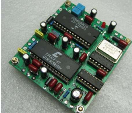
The development of electronics industry has promoted the development of PCB, but also to PCB manufacturing technology and surface mounting technology put forward higher requirements. The plug - hole technology came into being with the needs of The Times. PCB plug holes are usually placed on a second layer of ink after mask welding to fill heat dissipation holes, aperture less than 0.55mm.
PCB board to do the plug hole reason
Through hole is also called conductive hole. In order to meet customer requirements, the circuit board must be plugged conductive holes. After a lot of practice, the traditional aluminum plate plugging process is changed, and the white screen is used to complete the resistance welding plugging hole on the circuit board surface. Stable production and reliable quality.
The through hole acts as a connection and conduction line. The development of electronics industry has also promoted the development of PCB, and put forward higher requirements for PCB manufacturing technology and SMT processing technology. The perforated plug technology comes into being and needs to meet the following requirements:
1. Copper can be found in the through hole, but the plug cannot be used for resistance welding.
2. There must be tin lead in the through hole, with a certain thickness requirement (4 microns). Do not allow solder solder ink into the hole, resulting in tin beads hidden in the hole.
3. Through hole must be equipped with solder resistance ink plug hole, its light dense, Wuxi ring, tin bead, flatness and other requirements.
Five functions of a plug hole
1. Prevent short circuit on the surface of components caused by tin-penetrating through hole during wave soldering of PCB; Especially when we put through holes on BGA gaskets, we must make plug holes first, and then gold plating, so as to facilitate BGA welding.
2. Prevent flux from remaining in the through hole.
3. After completing SMT processing and component assembly in the electronics factory, the PCB must be vacuumed to form negative pressure on the testing machine.
4. Prevent the solder paste on the surface from flowing into the hole, causing false welding and affecting the installation.
5. Prevent soldering beads during wave soldering, resulting in short circuit.

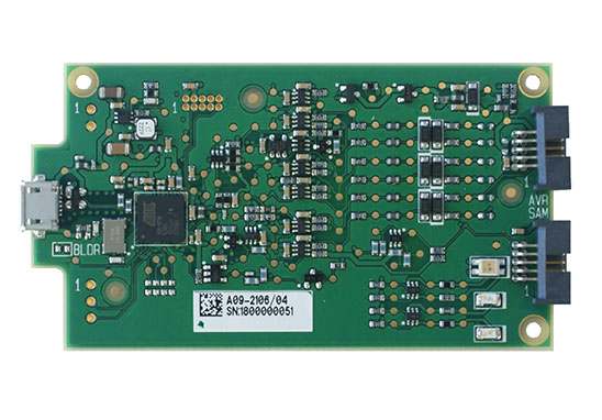
2. Precautions for selection of PCBA proofing components
In PCBA proofing, components with high sensitive voltage threshold should be used as far as possible on the premise of meeting the functional requirements of the circuit. Because the electrostatic and discharge sensitivity of a circuit board depends on the component with the lowest sensitive voltage threshold in the circuit board. Reasonable selection of components can effectively improve the success rate of PCBA proofing. Next, we will introduce matters for attention in selection of PCBA proofing components.
PCBA proofing components selection precautions
1, limit the output current, can avoid locking effect of CMOS circuit
The locking effect refers to the existence of parasitic PNP transistor and NPN transistor on the internal structure of CMOS circuit, and between them just constitute a parasitic PNPN thyristor structure. This interlocked positive feedback structure may be triggered by external factors (such as electrostatic discharge), and will flow current on the PNP tube (or NPN tube), and then through another parasitic NPN tube (or PNP tube) to amplify the current, and due to the positive feedback effect to make the current bigger and bigger and eventually burned out. It can be seen that limiting the current so that it cannot reach the level of maintaining the locking state is one of the problems to be considered for CMOS devices when PCBA proofing.
A common solution is to use a resistor to separate each output from its cable, and to use two high speed switching diodes to cable clamp the VDD (drain power supply) and VSS (source power supply).
2. Use filter network
Long input cables are sometimes required between the CMOS circuit system and the mechanical contacts, which increases the possibility of electromagnetic interference. A filter network should be considered. At the same time, a long input line must be accompanied by a large distributed capacitance and distributed inductance, which is easy to form LC self-excited oscillation, leading to the diode burn of the protection network. The solution is to connect a resistor in series at the input end, whose resistance value can be selected according to the formula R=VDD/1mA.
3. RC Network
Where feasible, for the sensitive input of bipolar devices, the effect of electrostatic discharge can be reduced by using a RC network of resistors with high resistance values and capacitors of at least 100pF.
4, avoid CMOS device input pin hanging
In PCBA proofing, the input end of CMOS devices welded to the circuit board should be avoided from being suspended. Also, note that all unused excess input leads on CMOS devices are not allowed to hang. This is because once the input terminal is suspended, the input potential will be in an unstable state, which will not only destroy the normal logic of the circuit, but also easily produce electrostatic breakdown, external noise interference and other phenomena. The redundant input terminal should be treated separately according to the function of the circuit.
Shenzhen kingford is committed to providing the best and fastest service for the continuous innovation of electronic technology, and becoming the first-class hardware outsourcing service provider in China. For global customers to provide professional PCB design, PCB board, SMT processing, PCBA OEM production (OEM supporting processing), PCB secondary development (can provide chip model identification and chip decryption) and other quality services.


Достаточно загрузить файлы Gerber, BOM и проектные документы, и команда KINGFORD предоставит полное предложение в течение 24 часов.