
Контрактное производство электроники под ключ в Китае
Шэньчжэнь, район Баоань, улица Фуюн, улица Фуцяо, район 3, промышленный парк Лонгхуй 6

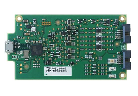
In PCBA processing, patch components and plug-in components are used. So what are the differences between patch components and plug-in components in PCBA processing? Next, Shenzhen PCBA processing manufacturer kingford will introduce you.
First, the difference between the two:
1. Patch components are small in size, light in weight, and easier to weld than plug-in components.
2, the patch element has a very important benefit, is to improve the stability and reliability of the circuit; Because the patch element has no leads, stray electric and magnetic fields are reduced, especially in high frequency analog circuits and high speed digital circuits.
2, the welding method of both
1. Welding method of patch components:
Put the component on the pad, apply the adjusted patch solder paste on the surface of the component and the contact point of the pad, and then use 20W internal heat electric soldering iron to heat the connection of the pad and the patch element (the temperature should be 220~230℃). After seeing the solder melt, you can remove the electric iron, and welding will be completed after the solder solidifies. After welding, you can use tweezers to clamp the welded patch element to see if there is any loosening. If there is no loosening, the welding is good. If there is any loosening, the solder paste should be applied again according to the above method of welding.
2. Welding methods of plug-in components:
When soldering all pins, solder the tips of the iron and apply flux to all pins to keep them moist. Touch the end of each pin of the chip with the tip of the soldering iron until the solder flows into the pin. After soldering all the pins, wet the pins with flux to clean the solder to eliminate any short circuits and lap joints. Finally, check with tweezers to see if there is any solder. After the check is complete, remove the flux from the circuit board. Dip the hard bristle brush with alcohol and wipe it carefully along the direction of the pins until the flux disappears.
2. How does PCB design determine the number of PCB layers?
The efficiency of PCB boards depends on the number of layers, so choosing the right number of layers is critical. So how does PCB design determine the number of layers? Next, kingford, a professional PCB design company in Shenzhen, will introduce you.
The following issues should be considered when deciding the number of PCB design layers:
1. Use
Where will the PCB be used? PCBS are used in a variety of types of simple to complex electronic devices. So the first thing to figure out is whether the application has minimal functionality or complex functionality.

2. Required signal type
The choice of layers also depends on the type of signal they need to transmit. Signals can be classified as high frequency, low frequency, ground or power. For applications that require multiple signal processing, multilayer PCBS are needed, and these circuits may require different grounding and isolation.
3. Through hole type
The choice of through-holes is another important factor to consider. If you choose to bury the through-holes, more internal layers may be required, so the multilayer requirements can be met accordingly.
4. Density and number of signal layers required
The PCB layer is also determined based on two important factors: signal layer and pin density. The number of layers in the PCB increases as the pin density decreases. Pin density is 1.0. For example, a pin density of 1 would require 2 signal layers. However, pin density. 0.2 May require 10 or more layers.
5. Number of planes required
The power and ground planes in the PCB help reduce EMI and shield the signal layer. Thus, the choice of layers will again depend on the number of planes required.
6. Manufacturing cost
Although a major requirement, it is one of the determining factors in choosing the number of layers in a 1-40 layer PCB design. The cost of PCB manufacturing depends on the multiple layers. Multilayer PCBS are more expensive than single-layer PCBS, and manufacturing costs will largely depend on the above requirements.
7. Delivery time
Delivery times based on 1-40 layer PCB designs depend on all of the above factors. For example, if your design requires a single layer, the lead time may be less. If you are ordering PCBS for complex industrial electronic equipment, the lead time will increase.
Usually PCB designers will determine how many layers of board design according to the complexity of the schematic diagram of the design circuit, mainly from the schematic diagram of the core device outlet and the difficulty of the layout of the device to decide. If you are unable to make a decision based on the above factors, it is best to discuss with the manufacturer.
kingford Co., Ltd. specializes in providing integrated PCBA electronic manufacturing services, including upstream electronic component procurement to PCB production and processing, SMT patches, DIP plug-ins, PCBA testing, finished product assembly and other one-stop services.
The company gives full play to its competitive advantages in scale procurement and quality control, and has signed long-term cooperation agreements with many electronic component manufacturers at home and abroad and around the world to ensure the quality and stable supply of raw materials, and transfer the benefits to customers.
Why are most PCB board colors green?
2023-03-03


Достаточно загрузить файлы Gerber, BOM и проектные документы, и команда KINGFORD предоставит полное предложение в течение 24 часов.