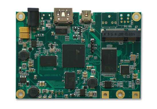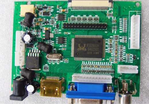
Solder resistance film is an important coating material in PCBA processing. It can provide medium and mechanical shielding for PCBA plate during and after welding, and prevent solder deposition in this position. Generally in the processing of electronic processing plants commonly used welding film has two kinds of materials, liquid and dry film.
Solder resistance ink is very important in PCBA processing and SMT patch processing. Its main role is to protect the circuit board, prevent the conductor from tin, prevent short circuit caused by moisture and other reasons, prevent the circuit breaker caused by unqualified contact mode in processing, and is one of the reasons to ensure that PCBA board can be used normally in harsh environment. The following Shenzhen PCBA processing plant for you to introduce PCBA processing welding resistance film common bad reasons
PCBA processing welding resistance film common causes of bad
1. Welding pad and through hole are connected. In principle, solder resistance should be applied to the wires between the mounting pads and the through holes.
2. Solder resistance design between pad and pad, solder resistance graphic specifications should conform to the design of welding end distribution of specific components; If the open window welding between the pad and the pad leads to short circuit between the pad during welding, the pad and the pad are designed to be independent of the pin welding mode, the pad will not short circuit between the welding.
3. Improper size of solder resistance graphics of components. Too large solder resistance graphic design will "shield" each other and lead to open welding, so that the spacing between components is too small.
4. There are holes under components without welding resistance film, and there are no welding resistance holes under components. The solder on the holes after wave soldering may affect the reliability of IC welding, and may also cause defects such as short circuit of components.

2. What do PCB positive and negative mean? What's the difference?
Many friends do not know PCB positive and negative is what? What's the difference? Shenzhen Honglijie Electronics is a professional PCB manufacturer, next for you a brief introduction.
Usually the solution used in the negative film process is an acid-base corrosion process. After film-making, the required path or copper surface is completely transparent, while the unwanted part is black. After the exposure of the route process, the completely transparent part will be chemically hardbotted due to the exposure of the dry film inhibitor to ultraviolet light, while the development process below will not harden the film, and the dry film will be washed away. Therefore, during the etching process, only the copper deposition of the part of the dry film washed away (the black part of the negative), while the preserved dry film is not washed away. This is the PCB board (the transparent part of the negative) we want.
What is a PCB positive?
Usually the positive process is based on alkaline etching process. On the negative, the desired path or copper surface is black, while the unwanted part is completely transparent. Similarly, after exposure to the route process, the completely transparent part is hardened by the chemical action of the dry film blocker exposed to ultraviolet light. The subsequent development process washes away the dry film without hard substrate in the next step. We remove the copper surface (the transparent part of the negative) without tin and lead maintenance with an alkaline solution, leaving the PCB board (black film) part.
The difference between PCB positive and negative
1. Distinguish screen printing screen plate (negative), working film, positive film and negative film and film surface: screen printing screen has master film and working film (subfilm), black and yellow film, positive and negative film;
2. Negative film is also called black film, also known as carbon negative. However, the working negative is not only the yellow film, but also the black film to make the work. It is mainly used for manufacturing high-precision HDI board or cost saving, in the small batch production of manufacturing PCB circuit boards in the one-time mass production and manufacturing PCB circuit board applications.
3. When the surface of the film is different, the bright side of the black film is the film, while the yellow film is the opposite. Generally, it can be seen that the side is based on the doodle pen or knife tip on the screen printing of the film surface.
4 yellow film application notes: smooth and matte two kinds of surface, the second kind of application is easy to appear oil surface indentation.
5. The negative film (containing copper) that transmits light on the membrane circuit is positive film; Positive film is used in graphic plating process, developer drop as the path, residual effect is corrosion resistant plating process, the key inlays are lead and tin. Films are usually used in the immediate etching process, corrosion resistance behind the developer is the way, and acid-base etching solution is used to carry out the immediate etching process.
kingfordPCBA processing capability
1. Maximum board card: 310mm*410mm(SMT);
2. Maximum plate thickness: 3mm;
3. Minimum plate thickness: 0.5mm;
4. Minimum Chip parts: 0201 package or parts above 0.6mm*0.3mm;
5. Maximum weight of mounted parts: 150g;
6. Maximum parts height: 25mm;
7. Maximum parts size: 150mm*150mm;
8. Minimum spacing of pin parts: 0.3mm;
9. Minimum ball parts (BGA) spacing: 0.3mm;
10. Minimum ball parts (BGA) ball diameter: 0.3mm;
11. Maximum parts mounting accuracy (100QFP) : 25um@IPC;
12. Patch capacity: 3-4 million points/day.
Our advantage
1. Strength assurance
- SMT workshop: With imported SMT machines and a variety of optical testing equipment, it can produce 4 million pieces per day. Every process is equipped with QC personnel who can keep a close eye on product quality.
- DIP production line: There are two wave welding machines. Among them, there are more than ten old employees who have worked for more than three years. Skilled workers can weld all kinds of insert materials.
2. Quality assurance, high cost-effective
- High-end equipment can mount precision heterosexual parts, BGA, QFN, 0201 materials. Proofing can be machine paste, also can be hand pendulum.
- Samples and large and small batches can be produced. Proofing starting price 800 yuan, batch starting price 0.008 yuan/point, no start-up fee.
3. Rich experience in SMT and welding of electronic products, stable delivery time
- Served thousands of home appliance subsidiaries, involved in various kinds of automotive equipment and industrial control motherboard SMT SMT processing services. Products are often exported to Europe and the United States, the quality of new and old customers affirmed.
- On time delivery, generally in 3 to 5 days after the board and material collection, small batch urgent can also be delivered on the same day.
4. Strong maintenance ability and perfect after-sales service
- Experienced maintenance engineers can repair defective products caused by various welding problems and ensure the connectivity rate of each circuit board.
- 24 hours customer service staff will be ready to respond and solve your order problems as soon as possible.


