
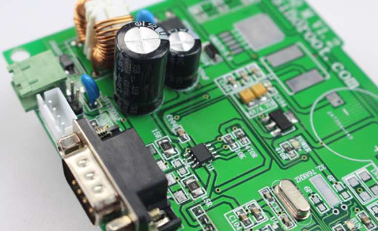
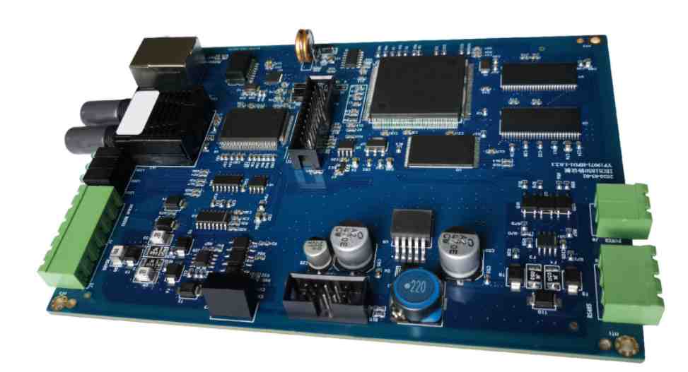
Контрактное производство электроники под ключ в Китае
Шэньчжэнь, район Баоань, улица Фуюн, улица Фуцяо, район 3, промышленный парк Лонгхуй 6

1. PCB size
The size of PCB is limited by the capability of the equipment in the electronic processing line, therefore, the appropriate size of PCB should be considered in the design of the product system scheme.
(1) The maximum PCB size available for SMT equipment is derived from the standard size of PCB board, most of which is 20 "×24", namely 508mm×610mm (width of guide rail).
(2) The recommended size is the matching size of each equipment in the SMT production line, which is conducive to the production efficiency of each equipment and the elimination of equipment bottleneck.
(3) For small size PCB should be designed into a Mosaic, in order to improve the production efficiency of the whole production line.
Design requirement
(1) Under normal circumstances, the maximum size of PCB should be limited to 460mm×610mm.
(2) The recommended size range is (200~250) mm× (250~350) mm, the aspect ratio should < 2.
(3) For size < 125mm×125mm PCB should be assembled to the appropriate size.
2. PCB appearance
SMT production equipment is to use guide rail to transfer PCB, can not transfer the irregular shape of PCB, especially the corner notch PCB.
Design requirement
(1) PCB shape should be regular square with four corners rounded.
(2) In order to ensure the stability of the transmission process, the irregular shape of PCB should be considered to convert it into a standard square by means of plate, especially the corner gap had better be completed, so as to avoid the plate in the transmission process of wave welding clamp claw.
(3) For pure SMT board, notch is allowed, but the notch size should be less than one-third of the length of the side where it is located. For more than this requirement, the design process edge should be completed.
(4) The chamfer design of gold finger in addition to the insertion side requires chamfer design, the two sides of the insert plate should also be designed with chamfer angles of (1~1.5) ×45°, so as to facilitate insertion.
3. Transfer side
The size of the transfer side depends on the requirements of the equipment's transfer guide rail, printing press, placement machine and reflow welding furnace, the general requirements of the transfer side above 3.5mm.
Design requirement
(1) In order to reduce the deformation of PCB during welding, the long side direction of non-assembled PCB is generally taken as the transmission direction; The direction of the long side should also be taken as the direction of transmission for the Mosaic.
(2) Generally, the two sides in the transmission direction of PCB or patchwork are used as the transmission edge. The minimum width of the transmission edge is 5.0mm. There should be no components or solder joints inside the front and back of the transmission edge.
(3) Non-transfer side, SMT equipment is not limited, it is best to reserve 2.5mm components forbidden area.
4. Positioning hole
Many processes, such as plate processing, assembly and testing, require accurate positioning of PCB, so the design of positioning holes is generally required.
Design requirement
(1) For each PCB, at least two positioning holes should be designed. One is designed to be circular and the other is designed to be long groove. The former is used for positioning and the latter for guiding.
There is no special requirement for positioning aperture, which can be designed according to the specifications of our own factory. The recommended diameter is 2.4mm and 3.0mm.
Positioning holes shall be nonmetallic holes. If the PCB is a blanking PCB, the positioning hole should be designed to strengthen the stiffness.
The length of the guide hole is usually 2 times the diameter.
The center of the positioning holes should be at least 5.0mm away from the transfer side. The two positioning holes should be as far apart as possible. It is recommended that the positioning holes be placed on the diagonal of the printed circuit board.
(2) For mixed PCB (PCBA with plug-in installed), the position of positioning holes had better be consistent with positive and negative, so that the design of the tooling can be common, such as the screw base can also be used for the tray of plug-in.
5. Positioning symbol
Modern SMT machine, printing press, optical inspection equipment (AOI), Solder Paste Inspection equipment (SPI), etc., all adopt optical positioning system. Therefore, optical positioning symbols must be designed on the PCB.
Design requirement
(1) Positioning symbols are divided into Global positioning symbols (Global Fiducial) and Local positioning symbols (Local Fiducial). The former is used for the positioning of the whole board, and the latter is used for the positioning of the plate sub-board or finely spaced components.
(2) The optical positioning symbol can be designed into square, diamond circle, cross shape, well shape, etc., the height of 2.0mm. It is generally recommended to design a circular copper definition figure of Ø1.0m, allowing for the contrast between the color of the material and the environment, allowing an open weld area 1mm larger than the optical positioning symbol, allowing no characters in it, and matching the presence or absence of copper foil underneath the three symbols on the same board.
(3) On the PCB surface with patch components, it is suggested to lay three optical positioning symbols for the whole board at the corner of the board, so as to carry out stereoscopic positioning of the PCB (three points determine a plane, and the thickness of the solder paste can be detected).
(4) For the Mosaic, in addition to three optical positioning symbols for the whole board, it is better to design two or three optical positioning symbols on the diagonal of each unit board.
(5) For QFP with lead center distance ≤0.5mm and BGA with center distance ≤0.8mm, the local optical positioning symbol should be set in the diagonal of the device, so as to accurately position it.
(6) If there are mounted components on both sides, then each side should have an optical positioning symbol.
(7) If there is no positioning hole on the PCB circuit board , the center of the optical positioning symbol should be more than 6.5mm away from the PCB transmission side. If there is a positioning hole on the PCB, the center of the optical positioning symbol should be designed near the center side of the positioning hole.


Достаточно загрузить файлы Gerber, BOM и проектные документы, и команда KINGFORD предоставит полное предложение в течение 24 часов.