
Контрактное производство электроники под ключ в Китае
Шэньчжэнь, район Баоань, улица Фуюн, улица Фуцяо, район 3, промышленный парк Лонгхуй 6

This paper analyzes the main manufacturing difficulties of high - level circuit board, such as the alignment between layers, inner line production, pressing production, drilling production and other technical difficulties. In view of the main production difficulties, the production control points of key processes such as interlayer alignment control, laminated structure design, inner line technology, laminated technology and drilling technology are introduced, which can be used for reference by peers.
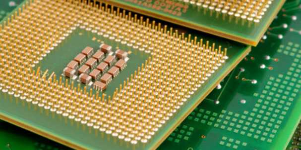
High level circuit board is generally defined as 10 layers ~ 20 layers or above high layer circuit board, more difficult than the traditional multi-layer circuit board processing, its high quality and reliability requirements, mainly used in communication equipment, high-end servers, medical electronics, aviation, industrial control, military and other fields. In recent years, the market demand for high-rise board in application communication, base station, aviation, military and other fields is still strong, and with the rapid development of China's telecom equipment market, the prospect of high-rise board market is promising.
At present, the domestic PCB manufacturers that can mass produce high - level circuit boards mainly come from foreign enterprises or a few domestic enterprises. The production of high level circuit board not only needs higher technology and equipment investment, more need technical personnel and production personnel experience accumulation, at the same time, the import of high level board customer certification procedures are strict and cumbersome, so the high level circuit board into the enterprise threshold, to achieve a long industrial production cycle. The average number of PCB layers has become an important technical index to measure the technical level and product structure of PCB enterprises. This paper briefly describes the main processing difficulties encountered in the production of high rise circuit board, introduces the control points of the key production process of high rise circuit board, for the peer reference and reference.
First, the main production difficulties
Compared with the characteristics of conventional circuit board products, the high level circuit board has thicker parts, more layers, more dense lines and holes, larger unit size, thinner dielectric layer and other characteristics, the inner space, the alignment between layers, impedance control and reliability requirements are more strict.
1.1 Difficulty of interlayer alignment
Due to the number of high-rise board layers, the customer design end of PCB layer alignment requirements are more and more strict, usually the inter-layer alignment tolerance control ±75μm, considering the large size design of high-rise board units, graphic transfer workshop ambient temperature and humidity, as well as different core board layer growth and shrinkage inconsistency caused by dislocation superposition, inter-layer positioning mode and other factors. It makes it more difficult to control the alignment degree between the layers of the high floor.
1.2 Difficulties in making inner circuits
High TG, high speed, high frequency, thick copper, thin dielectric layer and other special materials are used in high-rise board, which puts forward high requirements for inner line fabrication and graphic size control. For example, the integrity of impedance signal transmission increases the difficulty of inner line fabrication. Line width line distance is small, open short circuit increase, micro short increase, low qualified rate; There are more signal layers in the fine line, and the probability of missing AOI in the inner layer increases. Inner core plate thickness is thin, easy to fold resulting in poor exposure, etching machine is easy to roll plate; Most of the high-rise boards are system boards, the unit size is large, and the cost of scrap in finished products is relatively high.
1.3 Difficulties in pressing production
The superposition of multiple inner core plates and semi-cured sheets is easy to produce defects such as slide plate, delamination, resin cavity and bubble residue during pressing production. In the design of laminated structure, it is necessary to fully consider the heat resistance, voltage resistance, filling amount and medium thickness of the material, and set a reasonable high layer plate pressing program. Because of the large number of layers, the volume control and size coefficient compensation cannot be consistent. The thin insulation layer between layers is easy to cause the failure of inter-layer reliability test. FIG. 1 is the defect diagram of the layered burst plate after the thermal stress test.
1.4 Difficulties in drilling
Special plates of high TG, high speed, high frequency and thick copper are used to increase the roughness of drilling, burr of drilling and the difficulty of removing drilling dirt. The number of layers, the cumulative total copper thickness and plate thickness, drilling easy to break the knife; CAF failure caused by dense BGA and narrow pore wall spacing; The thickness of the plate is easy to lead to the problem of oblique drilling.
Ii. Control of key production processes
2.1 Material Selection
With the development of electronic components in the direction of high performance and multi-function, it also brings high frequency and high speed signal transmission. Therefore, low dielectric constant and dielectric loss of electronic circuit materials are required, as well as low CTE, low water absorption and better high-performance copper clad plate materials, in order to meet the processing and reliability requirements of high-rise board. Commonly used plate suppliers mainly include series A, Series B, Series C and series D. The main characteristics of these four kinds of inner substrate are compared, as shown in Table 1. For the high thickness copper circuit board with high resin content of the semi-cured sheet, the flow of the semi-cured sheet between layers is enough to fill the inner figure, the insulating medium layer is too thick easy to appear the finished plate super thick, on the other hand, the insulating medium layer is thin, easy to cause the quality problems such as dielectric layer, high pressure test failure, so the selection of insulating medium materials is very important.


Достаточно загрузить файлы Gerber, BOM и проектные документы, и команда KINGFORD предоставит полное предложение в течение 24 часов.