
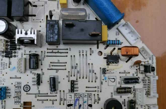
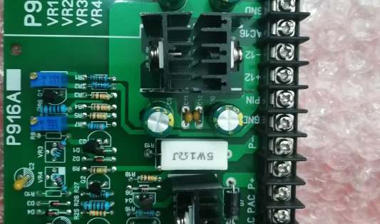
Контрактное производство электроники под ключ в Китае
Шэньчжэнь, район Баоань, улица Фуюн, улица Фуцяо, район 3, промышленный парк Лонгхуй 6

With the increasing popularity of plasma processing technology, the main functions in PCB process are as follows:
(1) Hole wall erosion/removal of hole wall resin drilling dirt
For the general FR-4 multilayer printed circuit board manufacturing, the CNC drilling after the removal of hole wall resin drilling dirt and pitting treatment, usually have concentrated sulfuric acid treatment, chromic acid treatment, alkaline potassium permanganate solution treatment and plasma treatment.
But for flexible PCB and rigid-flexible PCB to remove drilling dirt treatment, due to the different characteristics of the material, if the chemical treatment method is used, the effect is not ideal, and the use of plasma to drill dirt and dent, can obtain better roughness of the hole wall, conducive to the hole metallization electroplating, and at the same time has the "three-dimensional" dent connection characteristics.
(2) activation of PTFE materials
However, every engineer who has carried out the polytetrafluoroethylene material hole metallization manufacturing, have such experience: using the general FR-4 multi-layer printed circuit board hole metallization manufacturing method, is unable to get successful polytetrafluoroethylene printed circuit board hole metallization. The biggest difficulty is the pretreatment of teflon activation before copper deposition, which is also the most critical step.
There are a variety of methods can be used for the activation treatment of PTFE materials before the chemical precipitation of copper, but in summary, can achieve the guarantee of product quality and suitable for batch production, there are mainly the following two methods:

(A) Chemical treatment
Metallic sodium and naphthalene react in a non-aqueous solution such as tetrahydrofuran or ethylene glycol dimethyl ether to form a naphthalene sodium complex. The sodium naphthalene treatment solution can make the surface atoms of the polytetrafluoroethylene in the pore be etched, so as to achieve the purpose of wetting the pore wall. This is a classic successful method, good effect, stable quality, the most widely used.
(B) Plasma treatment
This method is a dry process, easy to operate, stable and reliable treatment quality, suitable for mass production. However, the sodium naphthalene solution treated by chemical method is difficult to synthesize, has high toxicity and short shelf life, and needs to be prepared according to the production situation, which has high safety requirements.
Therefore, at present, for the activation of PTFE surface treatment, most of the plasma treatment method, easy to operate, but also significantly reduce the treatment of wastewater.
(3) carbide removal
Plasma treatment, not only in all kinds of sheet material drilling decontamination effect is obvious, but also in composite resin materials and micro-hole drilling decontamination shows its superiority. In addition, with the increasing demand for higher interconnection density laminated multilayer printed circuit boards, laser technology is widely used to drill blind holes. As a product of laser drilling blind holes, carbon needs to be removed before the metallization process. At this point, plasma processing technology, without a doubt, takes on the task of removing carbide.
(4) Inner pretreatment
With the increasing demand of various kinds of printed circuit board manufacturing, higher and higher requirements are put forward to the corresponding processing technology. Among them, for flexible PCB and rigidly-flexible PCB inner pre-treatment, can increase the surface roughness and activity, improve the adhesion between the inner layers of the board, which is also very critical for successful manufacturing.
In this respect, plasma processing technology has shown its unique charm, and there are many successful examples. In addition, before the solder resistance film coating, the printed circuit board surface is treated by plasma, and a certain roughness and high activity surface can be obtained, so as to improve the adhesion of the solder resistance film.
(5) Residue removal
In terms of residue removal, plasma technology mainly has the following three functions:
(A) In PCB fabrication, especially in fine line fabrication, plasma is used to remove dry film residues/residual glue, etc., before etching to obtain a complete high quality wire pattern. If, once after development and before etching, anti-etching agent removal is not clean, it will lead to the occurrence of short circuit defects.
(B) Plasma treatment technology can also be used to remove residuals and improve weldability.
(C) For some special plates, the use of electroplating welderable coatings after graphic etching will cause shadow plating due to the presence of dirty copper particles etched on the edge of the line, which in severe cases will lead to product abandonment. At this time, plasma treatment technology can be used to remove fine particles of copper through ablation, and finally realize the processing of qualified products.


Достаточно загрузить файлы Gerber, BOM и проектные документы, и команда KINGFORD предоставит полное предложение в течение 24 часов.