
Контрактное производство электроники под ключ в Китае
Шэньчжэнь, район Баоань, улица Фуюн, улица Фуцяо, район 3, промышленный парк Лонгхуй 6

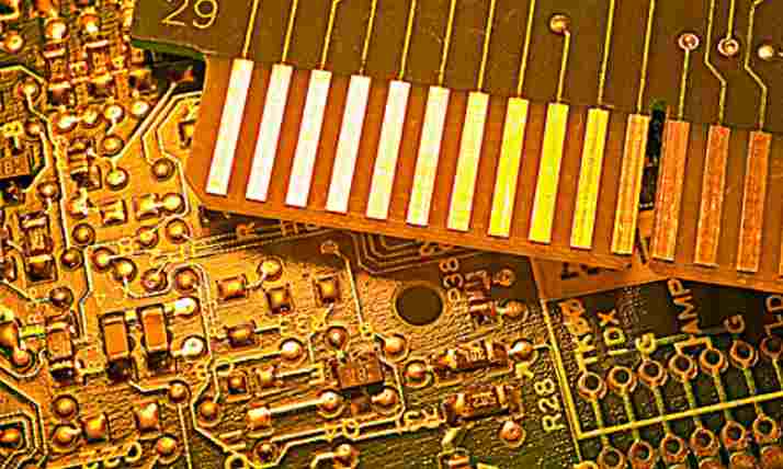
What are the differences between PCB layers?
In the design of PCB, many friends are not enough to understand the layer of PCB, especially novices, the role of each layer is more vague, this time we look at the use of software Altium Designer palette, what are the differences between the layers.
1. Signal layer
The signal Layer is divided into the Top Layer (top layer) and the Bottom Layer (bottom layer). This is the layer with electrical connections, which can place components and lay out cables.
2. Mechanical layer
Mechanical is the definition of the appearance of the whole PCB board. The emphasis on "mechanical" means that it has no electrical properties, so it can be safely used to outline the shape, outline the mechanical dimensions, place the text and so on, without worrying about any change in the electrical characteristics of the board. A maximum of 16 mechanical layers can be selected.
3. Screen printing layer
Top Overlay (top screen printing layer) and Bottom Overlay (bottom screen printing layer) are used to define the top layer and bottom screen printing characters, which are some text symbols printed on the solder resistance layer, such as component name, component symbol, component pin, copyright, etc., for convenience in future circuit welding and error checking.
4. Tin paste layer
The Paste layer includes the Top Paste layer and the Bottom Paste layer, which refers to the exposed surface of the solder pad that we can see, that is, the part of the solder paste that needs to be applied before welding. Therefore, this layer is also useful in hot air leveling of the pad and making welding steel mesh.
 5. Welding resistance layer
The Solder Solder layer is also often said to "open the window", including Top Solder and Bottom Solder, which is opposite to the solder paste layer, referring to the layer to cover the green oil. The layer does not stick to solder to prevent excess solder at adjacent welding points from short-circuiting during welding. The solder resistance layer covers the copper film wire to prevent the copper film from oxidizing too quickly in the air, but leaves a position at the solder joint and does not cover the solder joint.
Conventional copper coating or wiring is covered with green oil by default. If we deal with the corresponding welding resistance layer, it will prevent the green oil from covering and expose the copper.
6. Drilling layer
The Drill layers consist of Drill Gride(drill instruction Drawing) and Drill Drawing(drill drawing). The drill layers are used to provide information about the drill holes in the circuit board manufacturing process (e.g., solder pads, where holes are drilled).
7. No wiring layer
The Keep Out Layer is used to define the boundary of the wiring layer. After the keep out layer is defined, the wiring with electrical characteristics cannot exceed the boundary of the forbidden wiring layer in the future wiring process.
8. Multiple layers
The solder pad and through-hole on the circuit board need to penetrate the whole circuit board to establish electrical connection with different conductive graphic layers, so the system specially sets up an abstract layer-multilayer. Generally, the pad and the hole should be set on the multilayer, if the layer is closed, the pad and the hole can not be displayed.
High frequency and high speed board development prospect
Traditional copper-clad materials have high transmission loss and can not meet the requirements of high frequency signal transmission quality. Therefore, the most important performance of PCB substrate materials used in 5G communication is to meet the requirements of high frequency and high speed, as well as integration, miniaturization, lightweight, multi-function and high reliability. In particular, resin materials require low dielectric constant (Dk), low dielectric loss (Df), low thermal expansion coefficient (CTE) and high thermal conductivity. At present, the hard copper clad plate represented by polytetrafluoroethylene (PTFE) thermoplastic materials and hydrocarbon resin (PCH) thermosetting materials, because of its incomparable low dielectric properties occupy the majority of the high frequency/high speed PCB substrate market. In recent years, polyphenyl ether (PPO or PPE), bismaleimide (BMI), cyanate (CE), triazine resin (BT), benzoxazine (BOZ) and benzocyclobutene (BCB) and other new resin materials of high frequency/high speed PCB substrate. Polyphenyl ether (PPO or PPE), dielectric properties second only to PTFE, is the industry's attention in recent years. In addition, PPO materials are much better than PTFE materials in the workability, So at present, Very Low Loss (Very Low Loss) and Ultra low loss (Ultra Low Loss) in the high-speed plate are mainly modified PPO resin, such as Panasonic M6, M7N, Lianmao IT968, IT988GSE. The resin system of high frequency plate is mainly composed of polytetrafluoroethylene (PTFE) thermoplastic material and hydrocarbon resin (PCH). Although extremely low dielectric loss (Df) and stable dielectric constant (Dk) can be obtained, poor material machinability is not suitable for high multilayers, much less suitable
The processed products. With the development of 5G communication, PCB complexity of high-frequency products is also becoming higher and higher (traditional high-frequency PCB is mainly single and double sided, and the development of multilayer board even has HDI design requirements) in recent years, material developers also use PPO resin to make high-frequency board. To ensure the board has very low dielectric loss (Df) and stable dielectric constant (Dk) at the same time, to obtain good PCB processability. For example, Lianmao launched IT-88GMW, IT-8300GA, IT-8350G, IT-8338G, IT-8615G and other high-frequency plate is the use of modified PPO resin and hydrocarbon resin mixed system. While meeting the high frequency signal transmission requirements, the machinability of the material is greatly enhanced. On the one hand, the development of 5G communication towards higher speed and higher frequency will inevitably require the dielectric loss (Df) and dielectric constant (Dk) of materials to be smaller. On the other hand, 5G products require miniaturization and more unified PCB corresponding to the development of high multilayer or even HDI direction, which requires good machinability of materials. At present, the use of polyphenyl ether (PPO or PPE) resin is a good development direction, whether from high frequency materials or high speed materials.


Достаточно загрузить файлы Gerber, BOM и проектные документы, и команда KINGFORD предоставит полное предложение в течение 24 часов.