
Контрактное производство электроники под ключ в Китае
Шэньчжэнь, район Баоань, улица Фуюн, улица Фуцяо, район 3, промышленный парк Лонгхуй 6

Solder paste printing
The process of printing material onto a substrate using Screen printers, referred to as screen printing. It is used to leak solder paste or patch glue onto the solder pad of PCB to prepare for the welding of components. The equipment used is screen printing machine (screen printing machine), located at the front end of the SMT line.
Printing equipment: automatic printing machine, semi-automatic printing machine
Auxiliary materials: Solder paste, Adhesive
Tooling fixture: Stencil, Carrier
Printed object: Printed Circuit Board (PCB)
Fully automatic printing machine structure
1) Transport of PCB in the transmission system, that is, incoming, stop and outgoing functions.
2) Support the positioning system PCB, lift the fixed workbench, and fix the steel mesh.
3) The visual system recognizes the reference points of PCB and steel mesh, and compensates the positioning deviation through X and Y axes.
4) The printing system adheres the solder paste to the PCB evenly through the lifting, lowering and moving system of the scraper head.
5) The wiping system cleans the solder paste residue of the steel mesh through wet wiping, vacuum adsorption, dry wiping and other ways to prevent the mesh blockage of the steel mesh.
Auxiliary material
Tin paste
1) Ingredients of tin paste are listed below
2) Solder paste according to alloy composition
Lead Sn/Pb 63/37
Lead-free Sn/Ag/Cu 96.5/3.0/0.5
3) According to the particle size of tin powder
Type3 25-45um
Type4 20-38um
Type5 15-25um
4) The three characteristics of tin paste: fluidity, thixotropy and adhesion are the necessary conditions for realizing tin run printing.
5) Solder paste welding melting point: lead solder paste (Sn63/Pb37) welding melting point 183℃; Lead-free tin (SAC305) welding melting point 217 ~ 220℃.
6) Red glue is mainly used for auxiliary fixing of wave soldering process, but does not play the role of welding; The curing temperature of red glue is generally 150℃.
Tooling fixture
1) Steel mesh (PCB file or gerber file is required for making steel mesh)
Function: According to the PCB PAD hole. A template for applying solder paste to the surface of the PCB pad.
Manufacturing method: chemical etching, laser cutting, electric casting shape
Materials used: stainless steel, nylon, polyester.
Size: The commonly used mesh size is 37*47, 42*52, 55*65, 736*736. The steel mesh size is selected according to the PCB size and the size supported by the automatic printing press.
Thickness: Commonly used thickness 0.08mm, 0.1mm, 012mm, 013mm, 0.15mm. The choice of steel mesh thickness depends on the size of PCB pad and the precision of IC pin.
2) Vehicle
To flexible PCB(FPC) support or complex precision PCBA printing, patch, reflux play a bearing role, the general use of materials are synthetic stone, glass fiber board, aluminum alloy, etc.

Printed object
PCB, the purpose of printing is to attach the solder paste to the PCB pad.
Manufacturability design requirements for solder paste printing
1. PCB size requirements, conventional LW=50*50mm ~ 400*340m, T=0.5 ~ 4m.
2. The size is smaller than the minimum requirement, and the size of the plate should not be larger than the specification requirements of the printing press.
3. PCB front, PAD to board edge should be larger than 3mm, bottom support surface should be larger than 5mm, can not meet the need to add process edge.
4. The layout of FPC, thin board and BOT surface components is so dense that it is impossible to use the support PIN to support printing.
5. PCB weight is less than 1.5kg.
6. PCB surface welding plate layer needs to design a pair of Fidicial Mark, which is used for visual identification of equipment.
7. The general printing cycle of automatic printing press is 15 ~ 45sec. In the case of veneer patch material is not much, it is suggested to improve the efficiency of piecing board.
8. Automatic printing press acceptable steel mesh size 370*470 ~ 736*736mm.
9. PCB assembling board, the process should consider the smoothness of the direction of the flow plate. Generally, it is recommended that the aspect ratio should be greater than 1, at least 2:3.
10. PCB surface is smooth and clean, PCB warpage is less than 0.75%.
SPI: Solder Paste Inspection. Measure by structural light. Set a high-speed CCD camera in the vertical direction of PCB and solder paste, and irradiate periodic fringe light or image to PCB from the user projector at the Angle above. In the case of higher component on PCB, the image of fringe displacement relative to the base plane will be taken. Using the principle of triangulation, the offset value is converted into the height value, so that the solder paste printing is found in time before the patch and reflow welding, so as to avoid the unqualified PCB as far as possible, is a quality process control means.
Calculation method of volume: By measuring the height value in each pixel range, multiplying by the surface area of each pixel, cumulatively adding all the height values in the measured range, and very accurate volume can be obtained.
Volumetric method
SPI internal structure
Complete equipment drawing
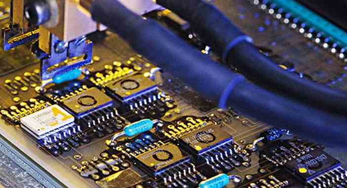
SMT machine: high speed SMT machine, multifunctional and high precision SMT machine.
2. Nozzle, Feeder
3. Components: ChipC/R, SOT, SOP, QFP, BGA and other packaging and patch devices.
4. Packing: braided tape, Tray.
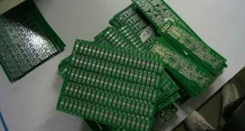
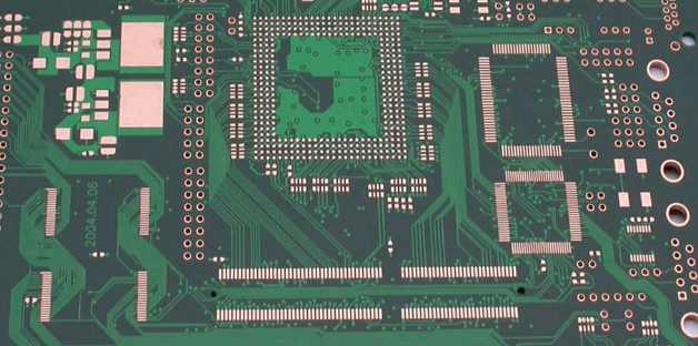
5. PCB, or printed circuit board, is an important electronic component, the support body of electronic components, and the electrical connection provider of electronic components. Because it is produced by electronic printing, it is called "printed" circuit board. Usually the PCB is green or brown in color, which is the color of Solder Mask. It's an insulating layer that protects the copper wire and prevents parts from being welded to the wrong place. A Silk Screen will also be printed on the solder resistance layer. It is usually printed with words and symbols (mostly white) to indicate the position of the parts on the board. PCB classification: According to the circuit layer classification: divided into single panel, double panel and multi-layer board. Common multilayer board is generally 4 or 6 layers, complex multilayer board can reach more than a dozen layers. According to the welding pad surface treatment classification: organic weldability protection layer (OSP), nickel metal leaching (ENIG), nickel palladium leaching (ENEPIG), silver Immersion silver, tin immersion.


Достаточно загрузить файлы Gerber, BOM и проектные документы, и команда KINGFORD предоставит полное предложение в течение 24 часов.