
Контрактное производство электроники под ключ в Китае
Шэньчжэнь, район Баоань, улица Фуюн, улица Фуцяо, район 3, промышленный парк Лонгхуй 6

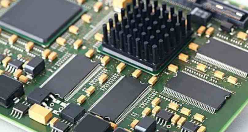
Today Xiaobian in tell friends a professional knowledge: PCBA processing, there is a lead process and lead-free process in the end what is the difference?
Lead technology has hundreds of years of development history, after a large number of lead technology experts research, with good welding reliability and stability, with mature production technology, which mainly depends on the characteristics of lead solder alloy.
Lead solder alloy low melting point, low welding temperature, less thermal damage to electronic products; Lead solder alloy wetting Angle is small, good weldability, product solder joint "false welding" possibility is small; The toughness of the solder alloy is good, and the vibration resistance of the solder joint is better than that of the lead-free solder joint.

Lead free welding process from the results of the present study to find alternative alloys with melting point temperatures are higher than existing tin lead alloys. For example, the "tin-silver-copper" alloy, which is likely to be widely accepted by the industry at present, has a melting point of 217℃, which will greatly narrow the process window in the welding process. Theoretically, the process window is reduced from 37℃ to 23℃ for solder solder. In fact, the shrinkage of the process window is much larger than the theoretical value. Due to the inaccuracy of our temperature measurement method in actual work, coupled with the limitation of DFM and the need to take good care of the "appearance" of the solder joint, the reflow welding process window is only about 14℃.
It is not only the narrowing of the process window that brings great challenges to the technicians, but also the increase of welding temperature that makes the welding process more difficult. One of them is oxidation during high temperature welding. As we all know, the oxide layer will make welding difficult, poor wetting, and cause virtual welding. In addition to adequate control over the incoming component itself, the required inventory conditions and time, the pre-processing (e.g. dehumidification and baking), and the heat energy (temperature and time) experienced during the preheating (or constant temperature) phase of the welding are all determining factors.
Because the lead-free process window is significantly smaller than the leaded process window, some in the industry believe that the use of nitrogen welding environments may be necessary. Nitrogen welding can reduce the surface tension of molten tin and increase its wettability. It also prevents oxidation during preheating. But nitrogen isn't a panacea. It can't solve all the problems of being lead-free. In particular, it is impossible to solve the problems that have been caused before the welding process.
In the current reflux welding equipment, the furnace design using the principle of forced hot air convection is the mainstream. Hot air convection technology is strong in the controllability of heating rate and constant temperature ability. It is weak in heating efficiency, heating uniformity and repeatability. These weaknesses are not serious in lead technology and are acceptable in many cases. With the narrowing of lead-free process window and the higher requirement of repeatability, hot air convection technology will be challenged.
How much is the temperature resistance of PCB circuit board?
In order to ensure the quality of finished PCB products, reliability and adaptability tests are required. The temperature resistance test of PCB circuit boards is to prevent adverse reactions such as board bursting, foaming and delamination at excessively high temperature, leading to poor product quality or direct scrap, which is a problem that needs to be paid attention to. So PCB circuit board temperature resistance is how much, how to do heat resistance test?
The temperature problem of PCB circuit board and its raw materials, solder paste, surface parts to withstand the temperature, usually PCB circuit board high temperature resistance of 300 degrees, 5-10 seconds; Over lead-free wave soldering temperature is about 260, over lead is about 240 degrees.
PCB circuit board heat resistance test:
1, first prepare PCB circuit board production board, tin furnace.
Sample 5 pieces of 10*10cm base plate (or pressed plate, finished plate); "(Copper-containing substrate without bubbling stratification).
Substrate: more than 10cycle; Pressed plate: LOW CTE 150 10cycle and above; HTg material more than 10cycle; Normal material at least 5 cycles.
Finished plate: LOW CTE 150 5cycle or above; HTg material more than 5cycle; Normal material at least 3 cycles.
2. Set the temperature of tin furnace at 288+/-5 degrees, and adopt contact temperature measurement and correction;
3, soak with a soft brush for flux, apply to the board face, reoccupy crucible 煹 pliers buccal test board into tin stove, timing out 10 SEC after cooling to room temperature, visual presence of foaming board appear, this is 1 cycle;
4. If the problem of bubbling and bursting plate is found visually, immediately stop leaching tin and analyze the initiation point f/m. If there is no problem, continue the cycle until the bursting plate, with 20 times as the end point;
5. It is necessary to slice and analyze the bubbling place, understand the source of detonation point, and take pictures.
PCB circuit boards will produce some bad problems in the overheating temperature, so for different materials of PCB circuit boards, the temperature resistance, need to be understood in detail, do not exceed its high limit temperature, so as to avoid the PCB circuit boards scrap, increase the cost.


Достаточно загрузить файлы Gerber, BOM и проектные документы, и команда KINGFORD предоставит полное предложение в течение 24 часов.