
Контрактное производство электроники под ключ в Китае
Шэньчжэнь, район Баоань, улица Фуюн, улица Фуцяо, район 3, промышленный парк Лонгхуй 6

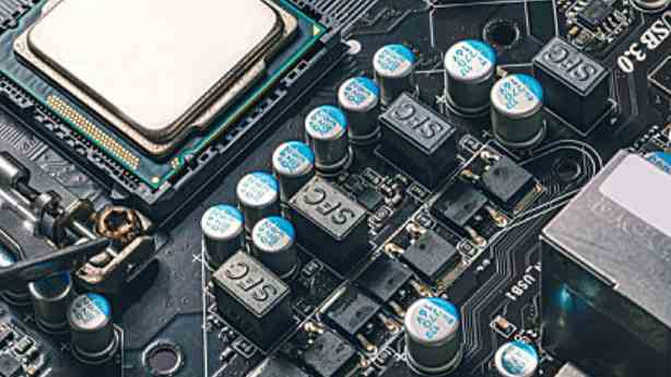
Gold-plated plate and gold-plated plate are often used in the process of PCB circuit boards, many engineers can not correctly distinguish the difference between the two, and even some engineers think that there is no difference between the two, this is a very wrong view, must be corrected in time. Next and you talk about the difference between PCB circuit boards and gold plating.
We all choose gold plating, what is gold plating, what we call the whole plate gold plating, generally refers to the "electric gold plating" "electroplating nickel gold plate" "electrolytic gold" "electric gold" "electric nickel gold plate", there is the distinction of soft gold and hard gold (general hard gold is used for gold finger), the principle is the nickel and gold (commonly known as gold salt) dissolve in chemical drops, The circuit board is immersed in the electroplating cylinder and connected to the current and the nickel gold coating is generated on the copper foil surface of the circuit board. The electronickel gold coating is widely used in electronic products because of the advantages of high hardness, abrasion resistance and oxidation resistance.
So what is the heavy gold? Gold deposition is through the chemical REDOX reaction method to generate a layer of coating, generally thick, is a kind of chemical nickel gold deposit method, can reach a thick gold layer.
The difference between the gold board and the gold plate:
1, the general gold for gold thickness is much thicker than gold plating, gold plating will be more yellow than gold, look at the surface of the customer is more satisfied with gold plating. These two forms a different crystal structure.
2. Because the crystal structure formed by sinking gold and gold-plating is different, sinking gold is easier to weld than gold-plating, which will not cause poor welding and cause customer complaints. At the same time, it is because the gold is softer than the gold, so the gold finger plate is generally gold-plated, hard gold wear-resistant.
3. There is only nickel gold on the solder plate, and the signal transmission in the skin effect is in the copper layer, which will not affect the signal.
4, gold plating is more dense crystal structure, not easy to produce oxidation.
5, with the wiring more and more dense, line width, spacing has reached 3-4MIL. Gilding is easy to produce gold wire short circuit. Gold plating only has nickel gold on the pad, so it will not produce gold wire short circuit.
6. Only nickel gold is deposited on the welding plate, so the welding resistance on the line is more solid with the copper layer. The work will not affect the spacing when compensating.
7, generally used for relatively high requirements of the board, the flatness is better, generally the use of gold, gold will not appear after the assembly of the black pad phenomenon. The flatness and service life of the gold plate are as good as those of the gold plate.
Bioneng belongs to Qinji Group, is the leading electronic industry service platform in China, providing online components, sensor procurement, PCB customization, BOM, material selection and other electronic industry supply chain solutions, one-stop to meet the comprehensive needs of small and medium-sized customers in the electronics industry.
The above is the difference between gold plate and gold plate, gold is expensive on the market now, in order to save costs many producers have been unwilling to produce gold plate, and only do nickel on the plate, the price is really cheap.
1, sinking gold plate and gold plate is the same process product, electric gold plate and flash gold plate is the same process product, in fact, it is just different people in the PCB industry of different names, sinking gold plate and electric gold plate is more in the mainland counterparts, and gold plate and flash gold plate is more in Taiwan counterparts.

2, the gold plate/gold plate is generally more formal known as the chemical nickel gold plate or nickel gold leaching plate, nickel/gold layer growth is the use of chemical deposition on the plating; Gold plate/flash gold plate is generally more formal called electroplating nickel gold plate or flash gold plate, nickel/gold layer growth is the use of direct current plating on the plating.
As the integration of IC becomes higher and higher, the IC feet are more and more dense. The vertical tin-spraying process is difficult to flatten the thin pad, which brings difficulties to SMT mounting. In addition, the shelf life of the tin spray plate is very short. And the gold-plated plate solves these problems:
1. In the trial production stage, influenced by components procurement and other factors, the board is often not welded immediately, but often has to wait for a few weeks or even a few months to use. The shelf life of the gold plate is many times longer than that of the lead tin alloy, so we are willing to use it. Moreover, the cost of gold-plated PCB at the sampling stage is almost the same as that of lead-tin alloy plate. But with more and more dense wiring, line width, spacing has reached 3-4MIL. So it brings the problem of short circuit of gold wire.
2, for the surface mounting process, especially for 0603 and 0402 ultra-small table paste, because the flatness of the welding pad is directly related to the quality of the solder paste printing process, and plays a decisive influence on the quality of the reflow welding behind, so the whole plate gold plating in high density and ultra-small table paste process often see.
With the increasing frequency of signal, the signal transmission in multiple coatings caused by skin effect has more and more obvious influence on signal quality
Skin effect refers to: high frequency alternating current, current will tend to concentrate on the surface of the wire flow. According to calculations, skin depth is related to frequency.
In order to solve the above problems of gold-plated plate, the use of gold-plated PCB has the following characteristics:
1. Because of the different crystal structure formed by sinking gold and gold plating, sinking gold will be more yellow than gold plating, and customers are more satisfied.
2, because the crystal structure formed by gold plating and gold plating is different, gold plating is easier to weld, will not cause poor welding, cause customer complaints.
3, because the gold plate only has nickel gold on the pad, the signal transmission in the skin effect is in the copper layer will not affect the signal.
4, the project will not affect the spacing when making compensation.
5, because the crystal structure is denser than gold plating, not easy to produce oxidation.
6, the flatness and service life of the gold plate is as good as that of the gold plate.
7, because the gold plate only has nickel gold on the pad, so it will not be produced into gold wire caused by short.
8, because the gold plate only has nickel gold on the welding plate, so the welding resistance on the line and the combination of copper layer is more firm.
9, because of the gold and gold plating formed by the crystal structure is not the same, the stress of the gold plate is easier to control, for the products of the state, more conducive to the processing of the state. At the same time, because the gold is softer than the gold, so the gold plate is not wear-resistant gold finger.


Достаточно загрузить файлы Gerber, BOM и проектные документы, и команда KINGFORD предоставит полное предложение в течение 24 часов.