
Контрактное производство электроники под ключ в Китае
Шэньчжэнь, район Баоань, улица Фуюн, улица Фуцяо, район 3, промышленный парк Лонгхуй 6


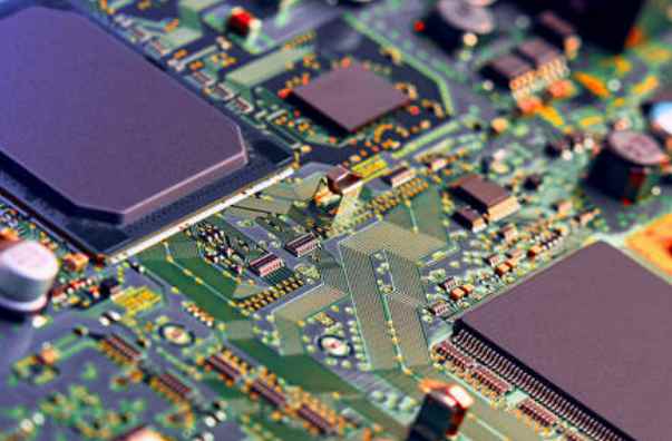
To eliminate RF currents in PCBS, the concept of flux cancellaTIon or flux minimization must be introduced first. Because the flux line in the transmission line runs in the reverse clock direction, if we make the RF return path parallel to and adjacent to the source line, the flux line on the return path (the field in the reverse clock direction) is compared to the source path (the field in the forward clock direction), they go in the opposite direction. When we combine the forward - clock - oriented field and the reverse - clock - oriented field, the effect of elimination can be produced.
If unwanted flux lines can be eliminated or minimized between the source end and the return path, radiating or conducting RF current does not exist except at the minimal boundary of the line. The concept of eliminating magnetic flux is simple, but there are pitfalls and omissions that must be noted when designing for elimination or minimization. Because of a small error, many additional errors can be caused, placing more debugging and debugging burden on EMC engineers. The simplest way to eliminate magnetic flux is to use the "image plane". No matter how well designed PCB wiring is, magnetic and electric fields are always present. However, if we eliminate the flux line, EMI does not exist. It's that simple!

In the design of PCB wiring, how to eliminate the flux line? There are many techniques available for reference, but not all of them are directly related to eliminating flux lines. Some of the techniques are summarized as follows:
The multilayer has the correct multilayer setup (stackup assignment) and impedance control.
clock trace is wound around the return path ground plane (multilayer PCB), ground grid, one side and two side panels can use ground trace, or guard trace.
The magnetic flux line generated inside the plastic package of the component is captured into the 0V reference system to reduce the radiation amount of the component.
Select logical components carefully to minimize the amount of RF spectrum distribution radiated by components and wires. A device with a slower edge rate can be used.
The on-line RF current is reduced by lowering the RF drive voltage (from the frequency generating circuit, e.g. TTL/CMOS).
Reduce the ground noise voltage, which is present in the power supply and ground plane structure.
When a maximum capacitance load must be pushed and the pins of all devices switched simultaneously, a decoupling circuit of the components must be sufficient.
Frequency and signal routing must be properly terminated to avoid ringing, overshoot and undershoot.
On selected networks, data line filters and common-mode choke are used.
Bypass (uncoupled) capacitors must be used correctly when external I/O cables are provided.
Provides a grounded heatsink (heatsink) for components that radiate large amounts of common-mode RF energy (generated within the component).
Looking at the items listed above, you can see that the flux line is only part of the reason why EMI is generated in the PCB. Other reasons:
There is a differential mode current between the circuit and the I/O cable.
The ground loop creates a magnetic field structure.
Components radiate.
Note that most EMI radiation is produced by common-mode quasi levels. In a circuit board or circuit, these common-mode levels may be converted into minimal fields.
To eliminate EMI in PCB, it is necessary to start with eliminating magnetic flux. But this is "easier said than done" because RF energy cannot be seen or heard. However, by finding the position and direction of flow of the RF current, using the techniques described in this article, and referring to Maxwell's equations, Kirchhoff and Ampere's laws, it is possible to gradually narrow down the suspicious area, find the correct EMI location, and eliminate it.
Why should the PCB board be blocked?
2023-03-29


Достаточно загрузить файлы Gerber, BOM и проектные документы, и команда KINGFORD предоставит полное предложение в течение 24 часов.