
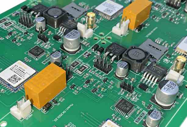
Контрактное производство электроники под ключ в Китае
Шэньчжэнь, район Баоань, улица Фуюн, улица Фуцяо, район 3, промышленный парк Лонгхуй 6

1. Opening principle: Cut aniseed into small pieces according to the size required by MI
2. Inner layer: Paste dry film or printing oil, exposure and etching film inner layer anticorrosion detection is a process of graphic transfer, through the use of film negative, ink/dry film and other media under ultraviolet light, the line graphics required by the customer will be made on the inner layer substrate, and then the unnecessary copper foil etching away, finally made into the inner layer of conductive lines. Pre-treatment: grinding plate inner dry film inner etching inner test + coarse copper plate surface, in order to increase the adhesion of the board and film + clean the board, get rid of the dry film and copper foil covering ink and copper foil covering
3. Plate pressing process: Browning, plate lining, pressing, X-RAY punching, hole and gong edge
4. Drilling process: The role of drilling: to produce a conductive channel on the circuit board that allows the later process to complete the connection between the upper/lower or intermediate circuit layers
5 wet process: copper sedimentation - outer dry film - graphic plating or plate plating - outer layer - corrosion plate - outer layer - corrosion copper detection action: deposit a layer of conductive copper layer on the hole wall of the circuit board insulation, conduction and the connection of the inner line. Outer dry film: stick dry film exposure image plating or plate plating: Function: increase the copper thickness of the circuit board hole \ wire \ face, so as to meet customer requirements. Outer etching: film retreat: The use of strong alkali can make the dry film dissolution or peeling properties of the unwanted dry film from the surface peel or dissolve corrosion plate: the use of bivalence copper ammonium and ion oxidation to the unwanted copper from the plate corrosion tin: The nitric acid in the tin removal water is used to react with tin to remove the tin layer from the board to the outer layer inspection :AOI&VRS takes the PCB image by CCD scanning, compares it with CAM standard graphics by computer and processes the logic of the design specification, marks the bad spots on the circuit board and sends the coordinates of the bad spots to the VRS, and finally confirms the bad spots Location.
6. Wet film process: the main process stations include: printing a layer of photosensitive ink on the outer wire board surface that has been formed and curing it, so as to protect the outer layer and insulation of the circuit board; pre-treatment grinding board, ink printing, oven exposure and image printing, character printing
7. Surface treatment process: Mainly according to the requirements of customers, the copper surface of the circuit board is processed by a layer. The main processing processes are: spray tin: spray a layer of weldable tin surface on the copper surface using hot air welding process. Tin sinking: The use of chemical principles through chemical treatment to deposit tin on the surface of the board. Silking: The depositing of silver on a surface by chemical processes
8. Sinking gold: Using chemical principles to deposit gold on the surface of the board through chemical principles. Gold plating: Using the principle of electroplating, through the current and voltage control of gold plating on the surface. Anti-oxidation: Using chemical principles to apply an anti-oxidation chemical to the surface 8. Molding process: Mainly according to the requirements of customers, will have formed a circuit board, processing into the size of the customer needs.
9. Open short circuit test inspection: mainly to check the open circuit and short circuit inspection of the line, as well as the use of visual inspection board quality.
10. Packaging and shipment: the qualified boards will be packaged and finally shipped to customers.

In order to study EDA technology and SCM technology in depth, the following keyboard, EDA technology and SCM technology application analysis, in order to effectively improve the technical level of software development, promote the long-term development of software development industry. In the study of EDA technology and single chip technology in the application of the keyboard, the use of EDA related software and programming download software, as well as the corresponding single chip microcomputer and supporting compilation software. Key board is generally selected matrix keyboard, has a wide range of practicability.
The application of EDA and single chip microcomputer in key board
In key board Settings, keys are set through the focus of the line and column lines, the two ends of the key switch and the line and column lines respectively connected. The connection of the line is through the pull-up resistance, so the line is in high level without any operation. When the key operation is carried out, the line will affect the level of the line, thus causing the change of the level of the line. The level of the line varies with the level of the column line. If the column line is high, the line is high. This is used in key recognition.
According to the key board key arrangement basis, in the use of EDA technology and single-chip technology, the matrix keyboard column line and line is used by the multi-key sharing, reduce the chip I/O interface possession, greatly improve the use of the keyboard speed. In the keyboard, the use of EDA technology and single-chip microcomputer technology to connect the signal, when the line and line affect each other, you can effectively control the key, to achieve the key closure. At the same time, through the combined application of EDA technology and SCM technology, can effectively control the switch of the keyboard, the keyboard operation at any time, so as to complete the corresponding work according to the relevant instructions.
EDA technology and SCM technology in the application of the keyboard, can help the keyboard to complete a variety of complex operations, in order to achieve effective control of the screen display, so as to switch different pictures, complete different tasks. The promotion and application of EDA technology and SCM technology in each industry, to the continuous improvement of economic benefits of each industry, promoting the long-term development of Chinese software industry, is of great significance for promoting the modernization construction of our country.
Chip heating
2023-03-26


Достаточно загрузить файлы Gerber, BOM и проектные документы, и команда KINGFORD предоставит полное предложение в течение 24 часов.