
Контрактное производство электроники под ключ в Китае
Шэньчжэнь, район Баоань, улица Фуюн, улица Фуцяо, район 3, промышленный парк Лонгхуй 6

kingf shared with us how to avoid mistakes when designing PCB!
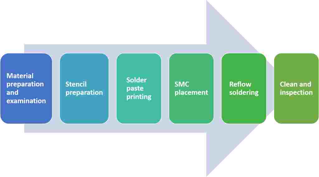
First, data input stage
1. Whether the data received in the process is complete (including: schematic diagram, *.brd file, material list, PCB design specification, PCB design or change requirements, standardization requirements, process design specification documents)
2. Make sure the PCB template is up to date
3. Check the position of the template positioning device
4.PCB design instructions, PCB design or change requirements and standardization requirements are clear
5. Ensure that the prohibited devices and wiring areas in the appearance diagram are reflected on the PCB template
6. Compare the outline drawing and confirm that the size and tolerance marked by PCB are correct, and the definition of metallized hole and nonmetallic hole is accurate
7. After confirming the accuracy of the PCB template, it is best to lock the structure file to avoid being moved by misoperation
Two, the layout after the inspection stage
a. Check the components
8. Confirm whether the package of all devices is consistent with the unified library of the company and whether the package library has been updated (use viewlog to check the running results). If not, be sure to Update Symbols
9. The mother board and the child board, and the board and the backplane must ensure that the signals and positions of the connectors are corresponding, that the connector direction and the silk screen mark are correct, and that the child board has anti-insertion measures, and that the devices on the child board and the mother board do not interfere
10. Whether the components are 100% placed
11. Open the place-bound of the TOP and BOTTOM layers of the device to see if DRC caused by overlap is allowed
12. Whether Mark points are sufficient and necessary
13. Heavier components should be placed close to PCB support points or support edges to reduce PCB warping
14. It is best to lock the device related to the structure after it is well distributed to prevent misoperation and move the position
15, Within 5mm around the crimp socket, there are no components whose height exceeds the height of the crimp socket on the front, and no components or solder joints are allowed on the back
16. Confirm whether the device layout meets the technology requirements (focusing on BGA, PLCC and patch socket).
17, metal shell components, pay special attention to not touch with other components, to leave enough space
18. Place the components related to the interface as close to the interface as possible, and place the backplane bus driver as close to the backplane connector as possible
19. Whether the CHIP devices of wave crest welding surface have been converted into wave crest welding package,
20. Whether there are more than 50 manual solder joints
21. Horizontal installation should be considered for axial insertion of higher components on PCB board. Allow for sleeping space. And consider the fixed mode, such as the fixed pad of crystal vibration
22. For the components that need heat sinks, ensure that they are sufficiently spaced from other components, and pay attention to the height of the main components within the heat sink range
b. Function check
23. Whether the digital circuit and analog circuit device layout of the digital-analog mixing board has been separated and whether the signal flow is reasonable
24, A/D converter is placed across the ADC partition.
25. Whether the layout of clock devices is reasonable
26. Whether the layout of high-speed signal devices is reasonable
27. Whether the terminal device has been placed reasonably (the matching string stop at the source end should be placed at the driver end of the signal; Intermediate matching string resistance placed in the middle position; The terminal matching string stop should be placed at the receiving end of the signal)
28. Whether the number and location of decoupling capacitors of IC devices are reasonable
29. The planes of different levels are used as reference planes for signal cables. When crossing the divided areas of planes, whether the connecting capacitors between reference planes are close to the routing area of signals.
30, whether the layout of the protection circuit is reasonable, whether it is conducive to segmentation
31. Whether the fuse of the board power supply is placed near the connector and there is no circuit element in front of it
32. Confirm that strong signal and weak signal (power difference 30dB) circuits are arranged separately
33. Whether devices that may affect EMC experiments are placed in accordance with design guidelines or reference to successful experience. For example, the reset circuit of the panel should be slightly close to the reset button
c. Fever
34. Keep heat-sensitive components (including liquid dielectric capacitor and crystal oscillator) away from high-power components, radiators and other heat sources as far as possible
35. Whether the layout meets the thermal design requirements and the heat dissipation channel (execute according to the process design document)
d. Power supply
36. Check whether the IC power supply is too far from the IC
37. Whether the layout of LDO and surrounding circuits is reasonable
38. Whether the circuit layout around the module power supply is reasonable
39. Whether the overall layout of the power supply is reasonable
e. Rule Settings
40. Whether all simulation constraints have been correctly added to the Constraint Manager
41, whether the physical and electrical rules are set correctly (note the constraint Settings of the power network and the ground network)
42. Test Via and Test whether the spacing of pins is sufficient
43. Whether the thickness and scheme of the lamination meet the design and processing requirements
44. Whether all differential line impedances with characteristic impedance requirements have been calculated and controlled by rules
Iii. Post-wiring inspection stage
f. Digital module
45. Whether the wiring of digital circuit and analog circuit has been separated and whether the signal flow is reasonable
46. If A/D, D/A, and similar circuits divide ground, does the signal line between the circuits run from the bridge between them (except the difference line)?
47. Signal lines that must cross the gap between divided power sources shall refer to the complete ground plane.
48. Ensure that digital signals and analog signals are routed in separate zones if undivided zones are used in the formation design. g. Clock and high speed parts
49. Whether the impedance of the high-speed signal line is consistent among all layers
51, make sure the clock line is as far inside as possible
52. Confirm whether the clock line, high-speed line, reset line and other strong radiation or sensitive lines have been wired according to the 3W principle as far as possible
53. Are there no forked test points on clock, interrupt, reset signal, 100 / gigabit Ethernet, high speed signal?
54. Is 10H between low-level signals such as LVDS and TTL/CMOS signals satisfied as far as possible (H is the height of signal line distance from reference plane)?
55. Do clock wires and high-speed signal wires avoid routing through dense through-hole areas or device pins?
56. Whether the clock line meets the requirements (SI constraint) (whether the clock signal is routed with fewer holes, short wires and continuous reference plane, the main reference plane is GND as far as possible; If the primary reference plane of GND is changed during layer change, it is the GND pass hole within 200mil from the pass hole.) If the primary reference plane of different levels is changed during layer change, is there a decoupling capacitor within 200mil from the pass hole?
57. Whether difference pairs, high-speed signal lines and all kinds of buses have met the (SI constraint) requirements
H.mc and reliability
58. For crystal vibration, is a layer of ground laid under it? Is signal line crossing between device pins avoided? For high speed sensitive devices, is the signal line traversing between device pins avoided?
59, the signal wiring of the board should not have acute angles and right angles (generally 135 degree Angle continuous turn, RF signal line is better to use circular arc or calculated Angle cutting copper foil)
60. For double panels, check whether the high-speed signal wire is wired closely together with its return ground wire; For multilayer panels, check that high-speed signal cables are routed as close to the ground as possible
61. Route signals at two adjacent layers as vertically as possible
62. Avoid signal cables passing under power modules, common-mode inductors, transformers, and filters
63. Try to avoid high-speed signals running parallel over long distances on the same level
64, plate edge and digital ground, analog ground, protection of the segmented edge are there shielded holes? Are multiple ground planes connected by holes? Is the hole distance less than 1/20 of the wavelength of the highest frequency signal?
65. Is the signal route corresponding to the surge suppression device short and thick on the surface?
66. Ensure that there are no isolated islands, large grooves, long ground plane cracks, slender strips, and narrow channels caused by large or dense through-hole isolation plates in the power supply and strata
67. Whether ground crossing holes are placed in areas where signal lines span more layers (at least two ground planes are required).
68. If the power/ground plane is divided, try to avoid high-speed signal crossing on the divided reference plane.
69. Ensure that the power supply and ground can carry sufficient current. Whether the number of holes through meet the load bearing requirements (estimation method: 1A/mm line width when the outer copper thickness is 1oz, 0.5A/mm line width in the inner layer, double the short current)
70. For the power supply with special requirements, whether the voltage drop requirements are met
71. In order to reduce the edge radiation effect of the plane, the 20H principle should be satisfied as far as possible between the power layer and the formation. (If conditions permit, the more indent the power layer, the better)
72. If ground is divided, does the divided ground not constitute a loop?
73. Is overlapping of different power planes in adjacent layers avoided?
74. Is the isolation of the protection ground, -48V ground and GND greater than 2mm?
75, Is the -48V ground only the -48V signal backflow, not connected to other places? If you cannot do this, please explain the reason in the remarks column.
76. Is there a 10-20 mm protective ground near the connector panel, and double rows of staggered holes are used to connect layers?
77. Check whether the distance between the power cable and other signal cables meets safety requirements.
78. In the case of metal shell devices and heat dissipation devices, there should be no wiring, copper and through holes that may cause short circuit
79. Mounting screws or washers should not be surrounded by wiring, copper and through holes that may cause short circuit
80. Whether the reserved position in the design requirements has cables
What might be the cause of pcb failure
2023-02-18


Достаточно загрузить файлы Gerber, BOM и проектные документы, и команда KINGFORD предоставит полное предложение в течение 24 часов.