
Контрактное производство электроники под ключ в Китае
Шэньчжэнь, район Баоань, улица Фуюн, улица Фуцяо, район 3, промышленный парк Лонгхуй 6

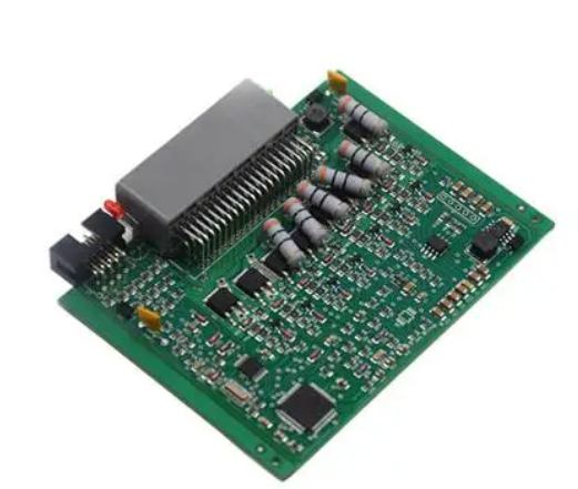
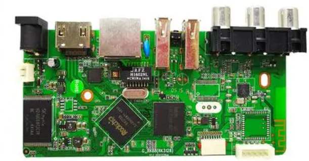
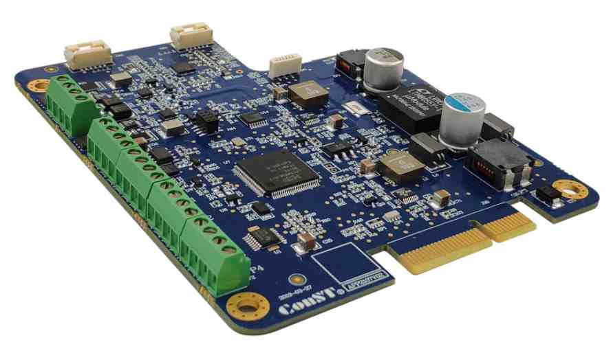
There are many production processes and raw materials in PCBA OEM. The circuit board is the core component of PCBA processing. What are the components of the circuit board? The following kingford to give you a brief introduction.
1. Welding pad:
The main form of the pad is the metal hole used to weld the pin of the component.
2. Number of layers:
PCB design according to the actual design will appear different layers of the circuit board, common such as double panel, 4 layers PCB design of board, 6 layers of board, 8 layers of board, the number of layers are generally even, in addition to the signal of the layer, there are other layers used to define processing.
3, through the hole:
The significance of through hole in actual production and processing is that if the circuit can not realize all signal routing at one level, it is necessary to connect the signal line through the hole. In PCBA foundry, perforations are generally divided into two types, one is metal perforations, the other is non-metal perforations, in which metal perforations are used to connect the pins of components between each layer. According to the process and model characteristics of PCBA processing plant can determine the form of hole and aperture.
4. Components:
PCBA is also the production process of welded components on PCB. The circuit board after welding can also be called PCBA. The wiring between the components and components can make the circuit board realize different functions.
5. Routing:
Wiring usually refers to the signal line between the pins of the connected devices on the circuit board. The length and width of the wiring depend on the nature of the signal, such as the size of the current, speed, etc., and the length and width of the wiring also vary.
6. Screen printing:
Screen printing can also be called screen printing layer, which is used to mark various information related to the device, such as bit number, board model, company name, etc. In PCBA foundry, silk screen printing is usually white, but different colors can also be selected according to the actual needs.
7. Welding resistance layer:
The main function of solder resistance layer is to protect PCB surface, form a protective layer with a certain thickness, and block the contact between copper and air. The solder stop layer is usually green, but there are also red, yellow, blue, white, and black solder stop layer options.
8. Positioning hole:
Positioning holes are holes for easy installation or debugging.
9. Fill:
The filling is used to apply copper to the ground network, which can effectively reduce the impedance.
10. Electrical boundary:
The electrical boundary is used to determine the size of the circuit board. All components on the circuit board cannot exceed this boundary.
kingford provides electronic OEM processing, PCBA processing plant, PCBA contract, SMT patch processing services.


Достаточно загрузить файлы Gerber, BOM и проектные документы, и команда KINGFORD предоставит полное предложение в течение 24 часов.