
Контрактное производство электроники под ключ в Китае
Шэньчжэнь, район Баоань, улица Фуюн, улица Фуцяо, район 3, промышленный парк Лонгхуй 6

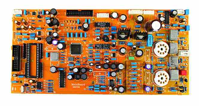
PCBa is a technology and processing technology popular in the electronic device assembly manufacturing industry at the present stage. It is a kind of surface assembled electronic devices without foot position or short conductor or ball drainage matrix sort package installed on the surface of pcb circuit board or other base steel plate surface, according to the reflow furnace or immersion welding and other ways of various electric welding assembly power circuit installation technology. The following patch processing manufacturer Xiaobian to explain how to prevent PCBA processing welding problems and how to improve the SMT patch processing efficiency related knowledge.
1. What are the processing steps of PCBA
Nowadays, many electronic device companies will submit their products to SMT patch processing manufacturers with professional technology for production and manufacturing. Generally, PCBA processing and sample determination will be made before mass production. Customers will place order information to SMT patch manufacturers with overall strength according to their specific requirements, and specify the actual regulations.
The SMT patch manufacturer will make an assessment according to its own working ability to see whether it can process the order information. After the customer decides to submit the order, he will present a series of documents and details to the SMT patch manufacturer, such as PCB electronic files, coordinates documents and BOM lists necessary for production and manufacturing. All these must be presented. Subsequently, the SMT patch manufacturer will purchase relevant raw materials from the opposite distributor according to the documents and materials presented by the customer for production and manufacturing sample determination.
The company undertakes :PCBA OEM, PCBA R & D design, SMT patch, DIP post-welding aging test, assembly and packaging, material procurement one-stop supporting services in the Pearl River Delta region industry the most professional PCBA OEM and PCBA R & D design company. The company has a strong global supply chain platform, can save costs for you; Strong engineering and technical team docking customers, timely solve problems, save time and worry; 13,000 square meters of dust-free production workshop, with strong manufacturing capacity, to provide customers with OEM/ODM services.

2. How to prevent PCBA machining welding problems
The porosity caused by PCBA welding, which is often called bubble, is generally manufactured according to the flow back welding and wave welding. In the process of packaging and printing of electronic devices, pcba samples are made by taking photos or electronic device color toner and have been properly modified, and printed as proof before packaging and printing of electronic devices or other ways to display the actual effect of information printing and platemaking. pcba is a technology and processing technology popular in the electronic device assembly manufacturing industry at the present stage. It is a kind of surface assembled electronic devices without foot position or short conductor or ball drainage matrix sort package installed on the surface of pcb circuit board or other base steel plate surface, according to the reflow furnace or immersion welding and other ways of various electric welding assembly power circuit installation technology. How to improve PCBA welding holes
① The PCB and parts will be exposed in the air for a long time to avoid moisture return.
(2) Control welding paste welding paste with moisture, very easy to cause skin pores and tin beads. Apply high quality solder paste. Strictly follow the temperature and mixing of solder paste according to the actual operation. Keep the solder paste exposed to air for as short a time as possible. Flow back welding must be performed immediately after packaging and printing of solder paste.
③ The environmental humidity control scheme of the production workshop detects that the environmental humidity control of the production workshop is in the middle of 4060%. pcba assembly has high relative density, small size and light weight of electronic equipment, and the volume and net weight of patch components can only be about 1/10 of the traditional plug-in components. Generally, after SMT is selected, the volume of electronic equipment will be reduced by 40% ~ 60%, and the net weight will be relieved by 60% ~ 80%.
(4) Set effective furnace temperature curve temperature control detection is carried out twice a day to improve the furnace temperature curve, and the heating speed can not be too fast. A technology and processing technology popular in the electronic device assembly manufacturing industry at the present stage, a surface assembled electronic device without feet or short conductor or ball drainage matrix ordering package is installed on the surface of the pcb circuit board or other base steel plate surface, The technology of power supply circuit assembly based on reflow furnace or dip welding.
⑤ welding aid spray painting in the recoating welding condition, flux can not be painted too much and spray painting is effective.
⑥ Improve the furnace temperature curve heating zone temperature should meet the requirements, not too low, so that the solution to evaporate completely, furnace speed can not be too fast. There will be many factors affecting the PCBA welding bubble, which can be analyzed from PCB design, PCB ambient humidity, temperature control, flux (spray paint specification), chain speed, tin wave height, welding material composition, etc.
What are the welding techniques of the patch
2023-02-12


Достаточно загрузить файлы Gerber, BOM и проектные документы, и команда KINGFORD предоставит полное предложение в течение 24 часов.