
Контрактное производство электроники под ключ в Китае
Шэньчжэнь, район Баоань, улица Фуюн, улица Фуцяо, район 3, промышленный парк Лонгхуй 6

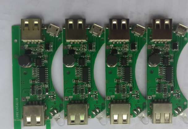
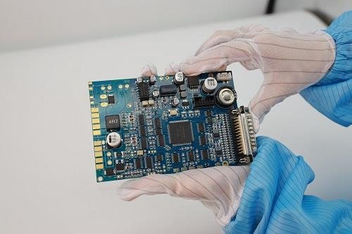
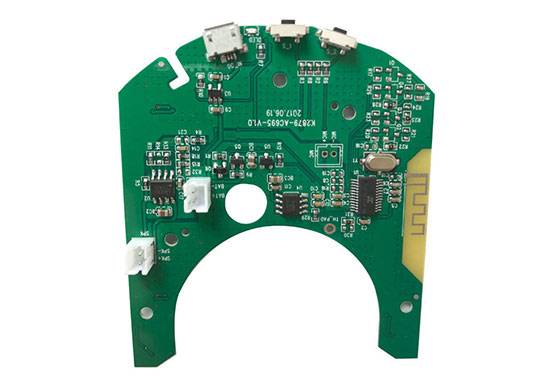
SMT patch processing is a very important process in electronic manufacturing. Now more and more circuit boards are produced and widely used. SMT patch assembly manufacturing involves many complex processes, and building it effectively can be very challenging.
Efficiency is essential in SMT patch processing. SMT factories can improve their overall productivity and even speed through scientific production management. You must pay attention to almost all factors related to SMT processing and assembly. Even the smallest point can lead to efficiency anomalies in assembly and manufacturing.
The installation speed of equipment indirectly depends on whether the assembly process is smooth. If SMT patch fabrication and assembly are inefficient, equipment problems may occur. There are a variety of methods and steps to improve the efficiency of circuit board manufacturing and assembly testing to produce perfect functional output.
Methods to improve SMT processing efficiency
1. Aim for fewer component changes
In the circuit board, you will see different components on the same board. Today, they play a very important role in the efficiency of SMT patch processing. Because, together, they are used to make the entire PCBA and thus to connect electrical functions.
Now, changes in these components can cause difficulties in the manufacturing process. It is important to note that different parts of a PCBA will differ if they come from different manufacturers. Not all manufacturers can produce the same components. Their components may vary - size, shape and function.
If there are complex and diverse categories of components, it is difficult to carry out efficient processing. In the process of patch processing, the fewer types of components, the better, the more unified brand model, the better, if there is any change should be as low as possible.
Ii. More focus on PCBA assembly (its manufacture and requirements)
If you do not know the requirements of PCB light board, how do you plan to improve the manufacturing efficiency of PCBA? Therefore, it is necessary to thoroughly understand the condition of PCB and work accordingly.
Here is where the manufacturing process comes in. You should focus on conducting the manufacturing process in a way that meets all the requirements of the PCBA. The PCB assembly manufacturing process should ensure that the output is efficient and of high quality.

You should know every step of the SMT process
Each step of the SMT process increases the importance of manufacturing. Various problems can arise during such steps and phases. There will be some difficulties in different processes, leading to quality problems and thermal properties. In this way, the production process may take more time, resulting in delayed delivery of the product. This can be risky because your reliability decreases.
None of these problems arise if you understand every step taken in the SMT process. It will help you point out where you went wrong and how to resolve those difficulties. This can help increase productivity, and your reliability will be right.
2.PCB design and layout secrets
After analyzing the principle of the entire circuit, you can begin to lay out the entire circuit. Next, Shenzhen PCB design company - Shenzhen kingford will introduce the ideas and principles of PCB design and layout to you.
PCB design layout ideas and principles
1. First of all, we will place the device with the required structure. When placing, according to the structure of the import, the connector must pay attention to the position of pin 1.
2, layout should pay attention to the structure of the height limit requirements.
3, if you want to layout beautiful, generally according to the component frame or center line coordinates to position (center alignment).
4, the overall layout should consider heat dissipation.
5, the layout of the need to consider the wiring channel evaluation, consider the length of the space required.
6. The layout needs to consider the power flow direction and evaluate the power channel.
7, high speed, medium speed, low speed circuit to separate.
8, strong current, high voltage, strong radiation components away from weak current, low voltage, sensitive components.
9, analog, digital, power supply, protection circuit to separate.
10, the interface protection device should be placed as close to the interface as possible.
11, interface protection device placement sequence requirements: (1) the general power surge protection device sequence is: varistor, fuse, suppression diode, EMI filter, inductance or common mode inductance, for the schematic missing above any device extension layout; (2) The general order of protection devices for interface signals is: ESD(TVS tube), isolation transformer, common-mode inductance, capacitance, resistance, for the schematic loss of any device layout; Strictly follow the order of the schematics (with the ability to judge whether the schematics are correct) to lay out the "font" layout.
12. The level conversion chip (such as RS232) is placed close to the connector (such as serial port).
13. Keep devices susceptible to ESD interference, such as NMOS and CMOS devices, away from areas susceptible to ESD interference (such as the edge of a board).
14, clock device layout: (1) crystal, crystal oscillator and clock distributor and related IC devices should be as close as possible; (2) The filter of the clock circuit (if possible, the filter of the "∏" type) should be close to the power input pin of the clock circuit; (3) Whether the output of crystal oscillator and clock distributor is connected with a 22 ohm resistor; (4) Whether the useless output pin of the clock distributor is grounded through the resistance; (5) The layout of crystal, crystal oscillator and clock distributor should be far away from high-power components, radiators and other heating devices; (6) Whether the distance between crystal vibration and plate edge and interface device is greater than 1inch.
15. Whether the switching power supply is far away from the AD/DA converter, simulator, sensitive device and clock device.
16, the switching power supply layout should be compact, input/output should be separated, in strict accordance with the requirements of the schematic layout, do not place the capacitor of the switching power supply at will.
17, capacitor and filter: (1) The capacitor must be placed close to the power pin, and the smaller the capacitance value of the more close to the power pin; (2) The EMI filter should be close to the input port of the chip power supply; (3) In principle, a 0.1uF small capacitor for each power pin and one or more 10uF large capacitors for an integrated circuit can be increased or decreased according to specific circumstances.
Why do you choose Shenzhen kingford for SMT processing?
1. Strength guarantee
▪SMT workshop: We have imported SMT machines and several sets of optical inspection equipment, with a daily output of 4 million. Each process is equipped with QC personnel, who can keep an eye on product quality.
▪DIP production line: We have two wave-soldering machines, among which there are more than 10 old employees who have worked for more than three years. The skilled workers can weld all kinds of plug-in materials.
2. Quality assurance, cost-effective
▪ High-end equipment can stick precision shaped parts, BGA, QFN, 0201 materials. Can also template patch, loose material hand.
▪ Sample and size batch can be produced, proofing from 800 yuan, batch 0.008 yuan/point, no start-up fee.
3. Rich experience in SMT and welding of electronic products, stable delivery
▪ Accumulated SMT SMT processing services for thousands of electronic enterprises, involving many kinds of automotive equipment and industrial control motherboard. The products are often exported to Europe and the United States, and the quality can be affirmed by new and old customers.
▪ On time delivery, normal 3-5 days after complete materials, small batch can also be expedited on the same day shipment.
4. Strong maintenance ability and perfect after-sales service
▪ Experienced maintenance engineers can repair all kinds of patch welding caused by bad products, to ensure the connection rate of each piece of circuit board.
▪ 24-hour customer service staff at any time response, the fastest speed to solve your order problems.


Достаточно загрузить файлы Gerber, BOM и проектные документы, и команда KINGFORD предоставит полное предложение в течение 24 часов.