
Контрактное производство электроники под ключ в Китае
Шэньчжэнь, район Баоань, улица Фуюн, улица Фуцяо, район 3, промышленный парк Лонгхуй 6

With the change of times, the transmission rate of high-speed PCB design wiring system is increasing, but it also brings a new challenge -- the anti-interference ability is becoming weaker. It all comes from the fact that the higher the frequency at which information is transmitted, the more sensitive the signal and the less powerful it is, the more susceptible the wiring system is to interference. In some common electronic devices, such as computer screens, mobile phones, electrical machines, and radio broadcasting devices, cables and devices may interfere with other components or be severely interfered by other interference sources. Next, Shenzhen kingford, a PCB design company in Shenzhen, introduces the shielding method in high frequency PCB design.
Shielding methods in high frequency PCB design
Especially when high-speed data networks are used, the time required to intercept large amounts of information is significantly lower than that required to intercept slow data transmission. The twisted-pair in data twisted pair can resist external interference and inter-pair crosstalk through its own twisting at low frequency, but at high frequency (especially when the frequency exceeds 250MHz), only twisting and merging can not achieve the purpose of anti-interference, only shielding can resist external interference.
The cable shield acts like a Faraday shield. Interference signals enter the shield, but not the conductor. As a result, data transfer can run without failure. Because shielded cables have lower radiation emission than unshielded cables, network transmission is blocked. Shielding networks (shielding cables and components) significantly reduce the radiation level of electromagnetic energy that may be intercepted when entering the surrounding environment.
The selection of shielding of different interference fields mainly includes electromagnetic interference and radio frequency interference. Electromagnetic interference (EMI) is mainly low frequency interference. Electric motors, fluorescent lamps, and power cords are common sources of electromagnetic interference. Radio frequency interference (RFI) refers to radio frequency interference, mainly high frequency interference. Radio, television broadcast, radar and other wireless communications are common sources of RF interference. For anti-electromagnetic interference, braided shielding is the most effective because of its low critical resistance; Foil shielding is the most effective for RF interference. Because braided shielding depends on the change of wave length, the gap generated by braided shielding allows high frequency signals to enter and leave the conductor freely. For high and low frequency mixed interference field, the combination of foil layer and braided net with broadband coverage should be used. Generally speaking, the higher the mesh shielding coverage, the better the shielding effect.

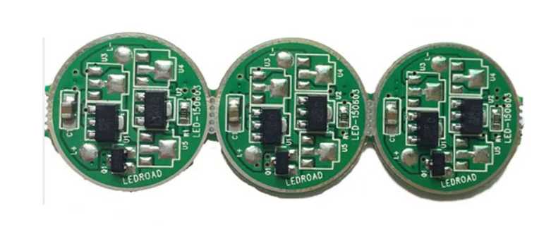
2. Why should PCBA process the board? What are the advantages of PCBA processing panels?
PCBA processing factory processing circuit board production will carry out a board operation, so why PCBA processing to the board? What are the advantages of PCBA processing panels?
Why should PCBA process the board?
PCBA processing and production of the plate operation problem, in the general PCBA processing factory processing circuit board production will carry out a splicing operation, no matter the PCBA processing plant or PCBA processing design, everyone needs to add the edge of the item, the purpose of this process is to increase the production efficiency of patch processing. Because the track of the SMT machine has a maximum and minimum size limit, for example, the maximum can pass through the 570mm*750mm size board, the minimum can pass through the 350mm*400mm size board. Not too big, not too small.
If you often go to the production workshop of PCBA processing plant, you can find this point. Moreover, the SMT patch processing currently consumes the most time is the solder paste printing link. First of all, the solder paste printing programming time does not say, is to brush the solder paste this process no matter how much the size of PCBA processing, so in order to ensure that the solder paste can be evenly coated on the PCBA processing welding paper, the printing time must be guaranteed at 20 seconds, because in contrast, to the SMT machine for component installation can play several components a second.
What are the advantages of PCBA processing panels?
PCBA machined pieceboard, if not pieceboard, even single sheet sub-size can pass through the placement machine track. But choose 1pcs, 1pcs, 1pcs such slow grinding, not only waste the production capacity of the SMT machine, but also irresponsible to the production efficiency. So if we integrate 10pcs, 20pcs,...... And so on. In order to improve the PCBA processing smooth plate printing solder paste and SMT patch in a short time of pasting through rate. With fewer wire changes, the circuit board spends less time on the track, which naturally increases efficiency. This maximizes the utility of a single device and improves the company's profit space.
PCBA processing of slabs also has the advantage of saving costs in another PCBA processing plant, because after the completion of processing, PCBA processing plant still needs a lot of testing and assembly, such as aging testing, burning testing, ICT testing, signal testing, etc., so the flow time in the production workshop is relatively large. It is also a big requirement for the storage space after patch processing. If it is plate storage, the tray may not be so much, and it can be tested even with the plate, and it can save the time wasted when the board is taken and placed in the fixture.
My company's PCBA processing capacity
1. Maximum board card: 310mm*410mm(SMT);
2. Maximum plate thickness: 3mm;
3. Minimum plate thickness: 0.5mm;
4. Minimum Chip parts: 0201 package or parts above 0.6mm*0.3mm;
5. Maximum weight of mounted parts: 150g;
6. Maximum parts height: 25mm;
7. Maximum parts size: 150mm*150mm;
8. Minimum spacing of pin parts: 0.3mm;
9. Minimum ball parts (BGA) spacing: 0.3mm;
10. Minimum ball parts (BGA) ball diameter: 0.3mm;
11. Maximum parts mounting accuracy (100QFP) : 25um@IPC;
12. Patch capacity: 3-4 million points/day.
Choose Shenzhen kingford do PCBA processing four reasons
1. Strength assurance
▪ SMT workshop: We have imported SMT machines and a variety of optical testing equipment, capable of producing 4 million pieces per day. Every process is equipped with QC personnel who can keep a close eye on product quality.
▪ DIP production line: There are two wave welding machines. Among them, there are more than ten old employees who have worked for more than three years. Skilled workers can weld all kinds of insert materials.
2. Quality assurance, high cost-effective
▪ High-end equipment can mount precision heterosexual parts, BGA, QFN, 0201 materials. Proofing can be machine paste, also can be hand pendulum.
▪ Samples and large and small batches can be produced. Proofing starting price 800 yuan, batch starting price 0.008 yuan/point, no start-up fee.
3. Rich experience in SMT and welding of electronic products, stable delivery time
▪ Has served thousands of home appliance subsidiaries, involving various kinds of automotive equipment and industrial control motherboard SMT SMT processing services. Products are often exported to Europe and the United States, the quality of new and old customers affirmed.
▪ On time delivery, usually within 3-5 days after the board is assembled, small batch expedited can also be shipped on the same day.
4. Strong maintenance ability and perfect after-sales service
▪ Experienced maintenance engineers are able to repair defective products caused by various welding problems and ensure the connectivity rate of each circuit board.
▪ 24-hour customer service staff will be ready to respond and resolve your order as soon as possible.


Достаточно загрузить файлы Gerber, BOM и проектные документы, и команда KINGFORD предоставит полное предложение в течение 24 часов.