
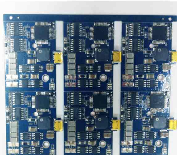
Контрактное производство электроники под ключ в Китае
Шэньчжэнь, район Баоань, улица Фуюн, улица Фуцяо, район 3, промышленный парк Лонгхуй 6


Common wiring rules for PCB design
1. Pre-divide the wiring area of digital, analog and DAA signals on the PCB board.
2. Digital and analog components and their corresponding wiring should be separated and placed in their respective wiring areas as far as possible.
3. Route high-speed digital signals as short as possible.
4. Route sensitive analog signals as short as possible.
5. Allocate power and land properly.
6. DGND, AGND, separate field.
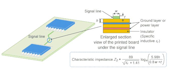
7. Use wide wires for power supply and critical signal routing.
8. The power cable and ground cable should be radial as far as possible, and the signal cable should not be looped back.
9. The digital circuit is placed near the parallel bus/serial DTE interface and the DAA circuit is placed near the telephone line interface.
10. Small discrete devices should be routed symmetrically. The leads of SMT pad with close spacing should be connected outside the pad, and direct connection in the middle of the pad is not allowed.
11. Key signal line priority: power supply, analog small signal, high-speed signal, clock signal and synchronization signal and other key signals priority.
12. The principle of routing density priority: Start wiring from the device with the most complex connection relationship on the board. Start wiring from the most densely wired area of the board.
13. PCB design should avoid sharp Angle and right Angle, produce unnecessary radiation, and PCB production process performance is not good.
14. There should be no through hole on the patch pad, so as to avoid the loss of welding paste and causing components

PCB design service process
1. The customer needs to provide data: schematic diagram (schdoc, DSN or sch) or netsheet, structure diagram (DXF), package library (to provide datasheet manual for new package), design requirements, etc.
2. Layout and wiring review: according to design specifications, design instructions, customer design requirements, and related CHECKLIST. After the project is started, our engineers will carry out DRC check of schematic diagram, structural check and other electrical design requirements. If there is any problem, we will immediately feedback and record EQ to the customer.
3. Customer layout confirmation: provide layout files and structure files for customers to review the layout; Customer confirms layout rationality, cascade scheme, impedance scheme, structure, packaging, and wiring parameters.
4. Design data output: PCB source files, Gerber files, assembly files, steel mesh files, structural files, etc. After the design of PCB Layout is completed, our engineers will carry out mutual inspection, including DFM inspection, QA inspection and EMC inspection. After the customer confirms OK, we will issue Gerber and other production documents.

2. The role of PCB design discharge teeth
What are discharge teeth?
Discharge tooth, also called discharge gap or spark gap. Discharge teeth are a pair of triangles pointing to each other at an acute Angle, which is made by using copper foil layer in PCB design and wiring process. These triangles shall be placed on another layer of PCB board components and shall not be covered by green oil.
The role of PCB design discharge teeth
During surge testing or ESD testing, high voltage will be generated at both ends of the common-mode inductor, resulting in flying arc. If the distance between the two devices is too close, the surrounding devices may be damaged. Therefore, a discharge tube can be connected to suppress its voltage. Such as gas discharge tube, parallel at both ends of the common-mode inductor, it can thus play an arc extinguishing effect.
Gas discharge tube has good inhibition effect, but the cost is relatively high. In many cases, we will place discharge teeth at both ends of the common-mode inductor in PCB design, so that the common-mode inductor can discharge through the tip of the discharge teeth, reduce or even avoid discharge through other paths, and protect the surrounding and post-stage devices.
This discharge tooth is through the form of air to discharge, so the design should pay attention to the different surface of the common mode inductance, although it can play a certain effect, but for often and surge current voltage, ESD in the occasion, if the use of this discharge tooth will be easy to produce carbon, a long time will cause short circuit, will go against the original intention of the design.


Достаточно загрузить файлы Gerber, BOM и проектные документы, и команда KINGFORD предоставит полное предложение в течение 24 часов.