
Контрактное производство электроники под ключ в Китае
Шэньчжэнь, район Баоань, улица Фуюн, улица Фуцяо, район 3, промышленный парк Лонгхуй 6

There are usually three manual welding methods for two end leadless chip components in SMT patch processing: spot welding one by spot, welding with special tools, and quick SMT patch welding with flat chip iron head.
Manual welding method for SMT patch processing of leadless chip components
One by one welding spot
(1) Hold the SMT component with tweezers, place the center paste on the corresponding welding basin, and hold it down with tweezers after alignment.
(2) Dip a fine brush in flux or use a welding aid pen to apply a small amount of flux on the welding pad at both ends.
(3) Add a little solder wire with a chisel-shaped (fill-shaped) iron head and a diameter less than or equal to 0.5mm. When the solder wire touches the iron head, it should leave quickly, otherwise the patch processing solder will add too much.
(4) First use the soldering iron head to heat one end of the pad about 25, and withdraw the soldering iron.
(5) Then heat the other end of the pad in the same way for about 2s and withdraw the soldering iron.
Note: During the welding process, the components should always be kept close to the pad to avoid the end of the components floating.
Two, the use of special tools horseshoe iron head welding
(1) Attach the component, and hold it down with tweezers after alignment.
(2) Apply a small amount of flux to the pad at both ends with a fine brush flux or a welding aid pen.
(3) Tin the horseshoe shaped iron head.
(4) Heat both ends of the pad at the same time with the horseshoe iron head for about 2s and withdraw the iron.
Three, the use of flat sheet iron head quick welding
(1) Attach the component, and hold it down with tweezers after alignment.
(2) Apply a small amount of flux to the pad at both ends with a fine brush flux or a welding aid pen.
(3) Tin the flat piece of soldering iron head.
(4) Heat both ends of the pad about 2 at the same time with the fan-shaped lattice iron head on the side of the element, and withdraw the soldering iron.
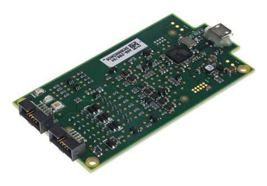
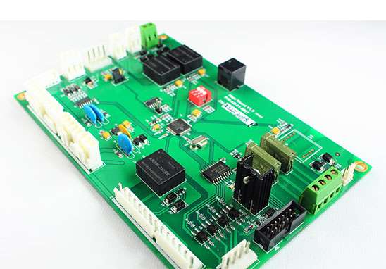
PCBA processing capability
1. Maximum board card: 310mm*410mm(SMT);
2. Maximum plate thickness: 3mm;
3. Minimum plate thickness: 0.5mm;
4. Minimum Chip parts: 0201 package or parts above 0.6mm*0.3mm;
5. Maximum weight of mounted parts: 150g;
6. Maximum parts height: 25mm;
7. Maximum parts size: 150mm*150mm;
8. Minimum spacing of pin parts: 0.3mm;
9. Minimum ball parts (BGA) spacing: 0.3mm;
10. Minimum ball parts (BGA) ball diameter: 0.3mm;
11. Maximum parts mounting accuracy (100QFP) : 25um@IPC;
12. Patch capacity: 3-4 million points/day.

2. Common rules of thumb in PCB routing design
The discussion of rules of thumb for PCB design is not about whether they are right or wrong. The problem is that the discussion often lacks context. This article tries to clarify the scenarios that these rules are adapted to, and tries to clarify when different rules are applicable and when they need to be avoided.
Common rules of thumb in PCB routing design
First, vertical wiring
The rule of vertical wiring is that the leads in adjacent signal layers need to be perpendicular to each other to reduce cross-talk caused by mutual inductance. In high frequency signals, crosstalk through capacitive coupling is the dominant component, producing current spikes between vertical leads.
When the signal changes along time, or the frequency is low (less than a few GHz), the coupling capacitance of the adjacent vertical wiring components of the signal layer has little interference. In the radio frequency (RF) band (tens of GHz), the interweaving of leads produces hole resonance, and the conductor structure that is not surrounded by ground wire will produce electromagnetic resonance at some special frequency points. This will cause strong crosstalk between the leads, even if they are perpendicular.
In order to eliminate interference at all frequency points, a simple and effective method is to use a multilayer board, using isolation layers between the signal layers. It is especially important in the application of high-speed signal change. When you are unsure about the strength of the coupling between orthogonal lines, you need to use basic crosstalk simulation software to check whether the crosstalk between the vertical leads is within the noise tolerance range. In this case, you need to plan the signal return path, which is a major problem in vertical wiring.
Two, heat dissipation hole
This is a classic "obey/avoid" rule that is often debated. Some PCB designers say they never use holes to prevent heat loss and never experience welding and assembly problems. And another group of people insist on preventing heat dissipation holes need to be used when each plane is connected. Which of them is right?
Their views are applicable to different situations. If you weld the circuit board manually, you need to increase the temperature of the soldering iron head to compensate for the heat dissipation caused by welding holes in the copper layer. But if you use wave welding, you need to use heat dissipation hole to prevent device loose, cold welding, monument and other phenomena, so I suggest you better bite the bullet and stick to the design of heat dissipation hole.
Three, right Angle wiring
This PCB routing rule is perhaps the most loved and hated of all. I still see a lot of PCB designers insisting that the wiring should not be angled at all times, for a variety of reasons. They say, for example, that it's hard for electrons to turn right angles as they move through the wires, but they don't want to think about the fact that all the holes in the circuit board are perpendicular to the wires. There are also some good reasons, such as the 45° corner to reduce the length of the lead, all right corner wiring needs to be chamfered. There is also the right Angle turning will produce acid corrosion trap in the circuit board acid corrosion solution, and there is no such problem in the widely used alkaline circuit board corrosion solution.
Unless your circuit board works in high frequency (millimeter wave radar /5G communications) circuits above 50GHz, you don't need to worry about the lead Angle. In fact, you can use any Angle you like when wiring the board. If you are using PCB design software with built-in electromagnetic field solving capabilities this will make wiring easier.
4. The "3W" Rule
Three rules of thumb for wiring. The first version of the "3W rule "states that the space between two adjacent leads should be at least three times the width of the leads in order to reduce the magnetic flux coupling between the leads and thus reduce the electromagnetic interference between the leads.
This rule may forget that the electromagnetic coupling between leads is proportional to the overlap area of the lead loops, not the distance between leads; Therefore, the overlap area of the lead loop is reduced, and the lead spacing is not restricted by the 3W rule. As with vertical wiring, basic EMI simulations can be used to examine the effects of different wiring spacing.
Another version of the "3W" rule states that when using sawtooth wiring for lead length matching, the sawtooth width must be at least three times the width of the lead, which minimizes discontinuity in lead impedance.
5. The 20H Rule
This rule defines the overlap distance between the ground layer and the power layer in the PCB. In modern PCB design, the power layer should be laid near the ground, so as to ensure sufficient interlayer capacitance between them, thus reducing the power fluctuation on the high-speed circuit board.
But the actual measurement turns out to be complicated. Some time results standard names at 300MHz follow the 20H rule can reduce electromagnetic radiation. However, there will be high-frequency resonance between the ground wire and the power supply layer, and their structure is similar to waveguide, which will aggravate the high-frequency interference between the lines.
So in practice, if your circuit is in the GHz range, you can follow the 20H rule. Otherwise, the 20H rule is likely to lead to worse results.
kingford is a professional PCB design company engaged in electronic products layout layout design, mainly undertake multi-layer, high density PCB design and circuit board design proofing business. Proficient in the use of market mainstream PCB design software, professional and efficient communication to ensure the progress of PCB design, to help you seize the market opportunity one step earlier!
SMT patch processing features
2023-02-23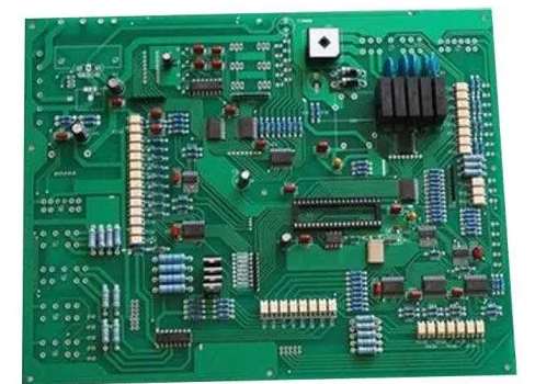


Достаточно загрузить файлы Gerber, BOM и проектные документы, и команда KINGFORD предоставит полное предложение в течение 24 часов.