
Контрактное производство электроники под ключ в Китае
Шэньчжэнь, район Баоань, улица Фуюн, улица Фуцяо, район 3, промышленный парк Лонгхуй 6

PCBA weldless pressing type connection technology, also known as pressing technology, is a kind of "moderate pressing" connection formed by elastic deformable connector or rigid connector embedded in double-sided or multi-layer printed board metallized hole, forming a close contact point between the connector and the metallized hole, electrical connection by mechanical connection.
The crimping technology has high reliability, plug safety and easy operation, avoiding the problem of large volume connector heat absorption during reflow welding, will not cause plug damage or fracture; At the same time, no solder and flux are needed to solve the problem of difficult cleaning and easy oxidation of welding surface. Therefore, the crimping technology continues today and is still widely accepted and used.
Key elements of PCBA crimp technology:
① press-in connector; ② Printed board; ③ crimping process; (4) Crimping tools and equipment
1. Press-in connector
Press-in connectors (press-in pins) are divided into rigid pins and flexible pins (see figure). Rigid pins do not deform during the crimping process, while holes will deform:
PCB rigidity and flexibility
Flexible pins will be squeezed and deformed in the process of crimping, but the hole will not be deformed
(1) Materials
A suitable grade of copper alloy shall be used for clamping. Such as copper tin alloy, bronze copper zinc alloy, brass or beryllium copper alloy.
The choice of materials depends not only on the size and function of the part but also on the requirements of having a good and stable electrical connection.
Stress relaxation occurs in all materials with respect to time, temperature and stress.
The end material and structure are such that the force holding the connection does not decrease so that the resistance at the connection increases to an unacceptable degree.
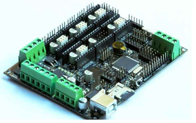
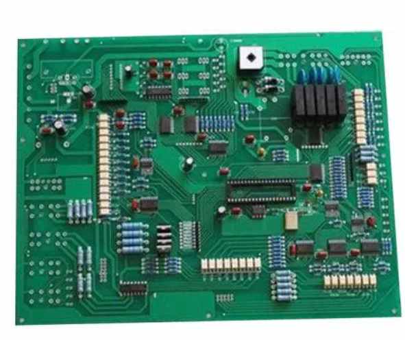
The whole PCBA processing process is a complicated and detailed process. Any quality problem of SMT patches or even PCB light board circuit board may cause product defects.

2. Prospect of SMC/SMD development trend
Surface Mounted Components/Surface Mounted Devices, abbreviated SMC/SMD (hereinafter referred to as SMC/SMD).
PCB Assembly components are also called chip components, chip components, surface mounted components. pcb assembly components refer to electronic components with rectangular sheet shape, cylindrical shape or opposite shape, no leads or short leads, whose welding ends or leads are made in the same plane and are suitable for SMT patch processing and assembly.
The development trend of SMC/SMD
Up to now, components used in SMT processing have been developed. SMC/ SMDS packaged in various types have been used in the production of electronic products, as shown in Figure 1. IC pin spacing has been developed from the initial 1.27mm to 0.8mm, 0.65mm, 0.4mm and 0.3mm. SMD devices have been developed from SOP (Small Outline Package) to BGA (Ball Grid Array). Ball grid array Package), CSP (Chip Scale Package), and FC (Flip Chip), whose guiding principle is still more and more I/0 and better and better reliability.
SMC/SMD
The emergence of new devices will inevitably bring many advantages. For example, CSP is not only a chip level package size, but also a high-quality chip that can be confirmed. It has the advantages of small size, light weight, ultra-thin (second only to FC), but there are also some problems, especially whether it can adapt to mass production. Although a device with a new package structure has infinite advantages, it cannot be called a good package if it cannot solve the problem of industrial production.
CSP is because of its complex production process, that is, the production needs to use microporous substrate, otherwise it is difficult to realize the interconnection of chip and component board, thus restricting its development. The trend of new IC packages is smaller size, more I/0, higher electrical performance, more reliable solder joints, better heat dissipation, and can achieve mass production.
Looking into the development trend of SMC/SMD in the future, it is not difficult to see that the progress of technology will inevitably give birth to new products, which will also inevitably promote the development of technology. The market of SMD/SMC is a vast blue ocean.a
The 20H principle in PCB design
2023-02-18


Достаточно загрузить файлы Gerber, BOM и проектные документы, и команда KINGFORD предоставит полное предложение в течение 24 часов.