
Контрактное производство электроники под ключ в Китае
Шэньчжэнь, район Баоань, улица Фуюн, улица Фуцяо, район 3, промышленный парк Лонгхуй 6

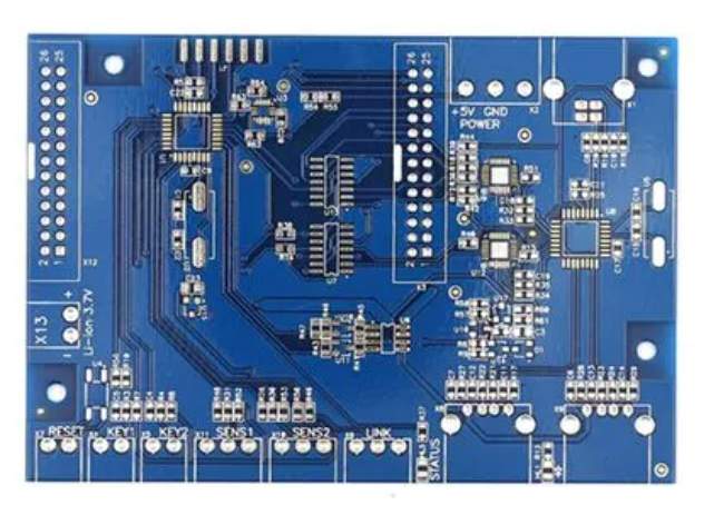
The technical realization process of PCB copying board is simply to scan the circuit board of the copying board, record the location of the components in detail, and then disassemble the components to make BOM and arrange material procurement. The empty board is scanned into pictures, processed by the copying software and restored to the PCB board drawing file, and then the PCB file is sent to the plate maker to make the board. After the board is made, the purchased components are welded to the PCB board, and then the circuit board is tested and debugged.
One, PCB copy board concrete steps
1. Get a PCB, first record the type, parameters and position of all the components on the paper, especially the direction of diode, three-stage tube and IC notch. It is best to take two pictures of the location of the key parts with a digital camera. Now the pcb circuit board more and more advanced above the diode triode some do not pay attention to see.
2. Remove all the multilayer plate copying parts, and remove the tin from the PAD hole. The PCB is cleaned with alcohol and placed in a scanner, which scans with slightly higher pixels to get a sharper image. Then the top and bottom layers are lightly polished with gauze paper until the copper film shines, put them in the scanner, start PHOTOSHOP, and sweep the two layers in color separately. Note that PCB board circuit must be placed horizontally and vertically in the scanner, otherwise the scanned image cannot be used.
3. Adjust the contrast and brightness of the canvas to make the contrast between the part with copper film and the part without copper film strong, then turn the subdrawing to black and white, check whether the lines are clear, if not, repeat this step. If it is clear, save the picture as black and white BMP format files TOP.BMP and BOT.BMP. If there is any problem with the picture, you can use PHOTOSHOP to repair and correct it.
4. Convert the two BMP files into PROTEL files respectively, and import two layers into PROTEL. If the positions of PAD and VIA after two layers are basically identical, it indicates that the previous steps have been done well. So pcb copy board is a very need patience, because a little problem will affect the quality and copy board after the matching degree.
5. Convert the BMP of the TOP layer to the TOP.PCB, pay attention to the SILK layer, that is, the yellow layer, then you trace the line on the TOP layer, and place the device according to the drawing of step 2. Delete the SILK layer when you are done. Repeat until all layers are drawn.
6. Import TOP.PCB and BOT.PCB in PROTEL, and it is OK to combine them into a figure.
7. Use a laser printer to print the TOP LAYER and BOTTOM LAYER onto the transparent film (1:1 ratio). Place the film on the PCB and compare it to see if it's wrong.
A copy of the original board was created, but it was only half done. But also to test, test copy board electronic technology performance is the same as the original board. If it's one, it's really done.
Remarks: If it is multi-layer board but also carefully polished to the inside of the inner layer, at the same time repeat the third to the fifth step of copying board steps, of course, the naming of the graphics are different, according to the number of layers, the general double panel copying board is much simpler than the multi-layer copying board, multi-layer copying board is prone to inaccurate situation, So the multilayer board copy board to be particularly careful and careful (which internal through holes and non-through holes are easy to appear problems).
Two, double panel copying plate method
1. Scan the upper and lower layers of the circuit board and save two BMP pictures.
2. Open the board copy software Quickpcb2005 and click "File" "Open base" to open a scanned image. Use PAGEUP to enlarge the screen, see the pad, place a pad according to PP, see the line line according to PT...... Just like a child's sketch, draw it in this software and click "Save" to generate a B2P file.
3. Click "File" and "Open base Map" to open another layer of scanning color map;
4. Click "File" "Open" again to open the previously saved B2P file. We can see the board we just copied, stacked on this picture -- the same PCB, the holes are in the same position, but the line connection is different. So we press "Options" - "Layer Settings", here to turn off the display of the top layer of lines and silk screen, leaving only multiple layers of holes.
5. The holes on the top layer are in the same position as the holes on the bottom picture. Now we can trace the bottom line as we did in childhood. Click "Save" again - the B2P file now has the top and bottom layers of data.
6. Click "File" "Export to PCB file", you can get a PCB file with two layers of data, which can be changed to the board or the schematic diagram or directly sent to the PCB platemaking factory for production.
Three, multi-layer board copying method
In fact, four layers of board copy board is repeated copy of two double panels, six layers is repeated copy of three double panels...... The reason the layers are so daunting is that we can't see the wiring inside. How do we see the inner workings of a sophisticated multilayer panel? -- Layering.
Now there are many ways to layer, there are potions corrosion, tool stripping, but it is easy to put the layer over, lost data. Experience tells us that sandpaper is the most accurate.
When we copy the top and bottom layer of PCB, we generally use sandpaper to grind off the surface layer to show the inner layer; Sandpaper is just plain sandpaper sold in hardware stores. Generally lay the PCB flat, then hold down the sandpaper and rub evenly over the PCB (if the board is small, you can also lay the sandpaper flat and rub the PCB over the sandpaper with one finger). The point is to smooth it so it's even.
Silk screen and green oil generally wipe off, copper wire and copper skin will be good to wipe a few times. Generally speaking, the Bluetooth board can be wiped in a few minutes, memory about ten minutes; Of course, it will take a little less time to work hard; It takes a little more time.
Grinding board is currently the most common scheme used in stratification, is also the most economical. We can find a piece of discarded PCB and try it. In fact, there is no technical difficulty in grinding the board, but it is a little boring. It takes a little effort, and you don't have to worry about wearing the board through to your fingers.
In the process of PCB layout, after the system layout is completed, the PCB drawing should be examined to see whether the layout of the system is reasonable and whether it can achieve the optimal effect.
Generally, it can be investigated from the following aspects:
1. Whether the system layout can ensure reasonable or optimal wiring, reliable wiring and reliable circuit operation. In the layout of the need to signal direction and power and ground network have an overall understanding and planning.
2. Whether the size of the printed board is consistent with the size of the processing drawings, whether it meets the requirements of the PCB manufacturing process, and whether there is a behavior mark. This point needs special attention, many PCB layout and wiring are designed very beautiful and reasonable, but the precise positioning of the positioning plug-in is neglected, resulting in the design of the circuit can not be connected with other circuits.
3. There is no conflict between components in two-dimensional and three-dimensional space. Note the actual size of the device, especially the height of the device. In the welding of the free layout of the element device, the height generally cannot exceed 3mm.
4. Whether the component layout is dense and orderly, arranged neatly, and whether all the cloth is finished. In the Layout of components, it is not only necessary to consider the direction and type of signals, the places that need attention or protection, but also to consider the overall density of the device layout, so as to achieve uniform density.
5. The components that need to be replaced frequently can be easily replaced, and the plug-in board can be easily inserted into the equipment. The convenience and reliability of the replacement and insertion of frequently replaced components shall be ensured.


Достаточно загрузить файлы Gerber, BOM и проектные документы, и команда KINGFORD предоставит полное предложение в течение 24 часов.