
Контрактное производство электроники под ключ в Китае
Шэньчжэнь, район Баоань, улица Фуюн, улица Фуцяо, район 3, промышленный парк Лонгхуй 6

Surface treatment technology
At present, the environmental problems involved in PCBA production are particularly prominent. Lead and bromine are the hottest topics right now. Lead-free halogen will affect the development of PCB in many ways. Although the current changes in PCBA surface treatment processes are not significant and seem relatively distant, it is important to note that long and slow changes can make a big difference. With the increase of environmental problems, PCBA surface treatment technology is bound to change dramatically in the future.
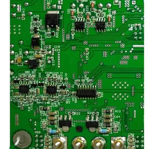
PCB surface finish is the coating between the component and bare board PCB. It is used for two basic reasons: to ensure solderability and to protect exposed copper circuits. As there are many types of finish, choosing the right finish is no easy task, especially as surface mounting has become more complex and regulations such as RoHS and WEEE have changed industry standards.
HASL (Hot Air Solder Leveling) /HASL Lead-free:
Hot air solder leveling is the PCB surface coated with molten tin lead solder and heated compressed air leveling (blowing), so that it forms a layer of copper oxidation resistance and good solderability of the coating. PCB circuit board should be immersed in molten solder during hot air solder leveling. The air knife rinses the liquid solder before it sets, minimizing the crescent shape of the solder on the copper surface and preventing welding Bridges.
Hot air rectifier is divided into vertical and horizontal two kinds. Generally speaking, horizontal is better, horizontal hot air leveling coating to uniform. The general process of automatic production is as follows: micro corrosion → preheating → flux coating → tin-spraying → cleaning.
Advantages: Low cost, available, repairable
Disadvantages: Uneven surface, not suitable for fine-spaced components, thermal shock, not suitable for electroplating through hole (PTH), poor wettability
Organic Coating (OSP) :
Unlike other surface treatment processes, OSPs act as a barrier between the copper and the air. Simply put, OSP is the chemical process of growing a layer of organic skin film on the surface of clean bare copper. It is resistant to oxidation, heat shock and moisture and protects the surface of copper from rust (oxidation or vulcanization, etc.). In a normal environment. At the same time, at the welding temperature after welding, it must be easily cleaned by flux. The simple process and low cost of organic coating make it widely used in industry. Early organic paint molecules were antirust imidazole and benzotriazole, and more recent molecules are mostly benzoidazole. In order to guarantee multiple reflow, it may not be possible if the copper has only one organic coating on the surface, that is, there must be many organic layers, which is why copper solutions are often added to the chemical bath. After the first coating, the coating adsorbs the copper. Then, a second layer of organic coating molecules binds to the copper until twenty or even hundreds of organic coating molecules are concentrated on the surface of the copper.
The general process is: degreasing → micro-etching → pickling → pure water cleaning → organic coating → cleaning, which is much easier than other processing processes.
Advantages: Lead-free, flat, simple process, repairable
Disadvantages: Adverse to PTH, sensitive, short shelf life
ENIG (Electroless nickel plating/gold plating) :
Unlike OSP, ENIG is just a thick nickel-gold alloy with excellent electrical properties on the surface of copper. It can protect PCB for a long time and act as an antirust layer. It can play a role in the long-term use of printed circuit board and achieve good electrical properties. More importantly, it also has environmental tolerance that other surface treatments do not have. Nickel plating occurs because gold and copper spread out from each other, and the nickel layer prevents them from spreading out. Without the nickel layer, the gold would spread to the copper within hours. Another benefit of electroless nickel plating/dipping is the strength of nickel, which is only 5um thick and allows controlled Z expansion at high temperatures. In addition, electroless nickel/gold plating also prevents copper from dissolving, which will facilitate lead-free welding.
The general process is pickling cleaning → microetching → preleaching → activation → electroless nickel plating → chemical leaching. The whole process, with six chemical tanks and nearly 100 chemicals involved, is relatively complex
Pros: Flat, sturdy, lead-free, suitable for PTH
Cons: Black pad syndrome, expensive, not suitable for remaking
Sunken silver:
The difficulty of silver impregnation process in SMT production is between OSP and electroless nickel plating. Silver immersion does not coat PCBS with heavy armor, provides excellent electrical properties and maintains good weldability even in hot, wet and polluted environments, but tarnishes. Since there is no nickel beneath the silver layer, silver immersion does not have all the good physical strength required for ENIG. Silver immersion is a displacement reaction, almost submicron level of sterling silver coating. Sometimes organic matter is included in the process, mainly to prevent silver corrosion and eliminate silver migration problems. In general, it is difficult to measure organic matter in this thin layer, and analysis suggests that it is less than 1% by weight.
Tin immersion:
Since all current solder is tin-based, the solder layer can match any type of solder. However, the previous PCB board impregnation process is prone to produce tin whiskers, and the transfer of tin and tin during welding will bring some unavoidable problems, thus limiting the use of impregnation process. After adding organic additives to the solution, the tin layer has a granular structure, which overcomes the previous problems and has good thermal stability and weldability.
Tin dipping process can form flat copper-tin compounds, with good solderability, as hot air leveling, but there is no flatness problem. There is no diffusion problem between electroless nickel plating and impregnated metal, except that the tin plate cannot be soaked for too long.


Достаточно загрузить файлы Gerber, BOM и проектные документы, и команда KINGFORD предоставит полное предложение в течение 24 часов.