
Контрактное производство электроники под ключ в Китае
Шэньчжэнь, район Баоань, улица Фуюн, улица Фуцяо, район 3, промышленный парк Лонгхуй 6

SMT patch processing is a very complex process, including a lot of technical processes, need to work carefully, otherwise there will be bad products, for you to introduce the SMT patch process in the most detailed process:
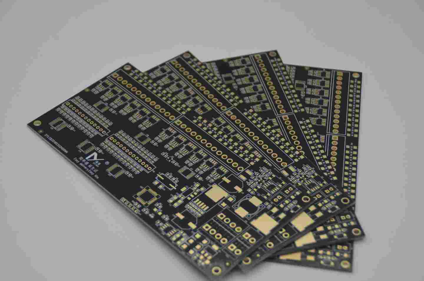
1. PCB Mosaic board
In the process of PCB board assembling, the most important thing to pay attention to is the problem of cutting PCB patch after processing. Due to the reason of production cost, many PCB manufacturers adopt manual board parting, resulting in the increase of labor cost. Nowadays, the electronic products on the market have higher and higher requirements on the volume and size. The thinner PCB is, the easier it is to deform after being subjected to external force. If there are too many pieces of board, the whole area of the board will become very wide.
2, three anti-paint coating
Three anti-paint coating is the last link of SMT patch. If there is no mistake in the previous welding and testing assembly, we can ship after this process is completed. Manual coating and machine spraying are two common three anti paint coating methods, manual coating is suitable for small batch, random, machine coating for large quantities, mainly in accordance with the preset program spraying, can effectively prevent the quality of the poor due to artificial mistakes.
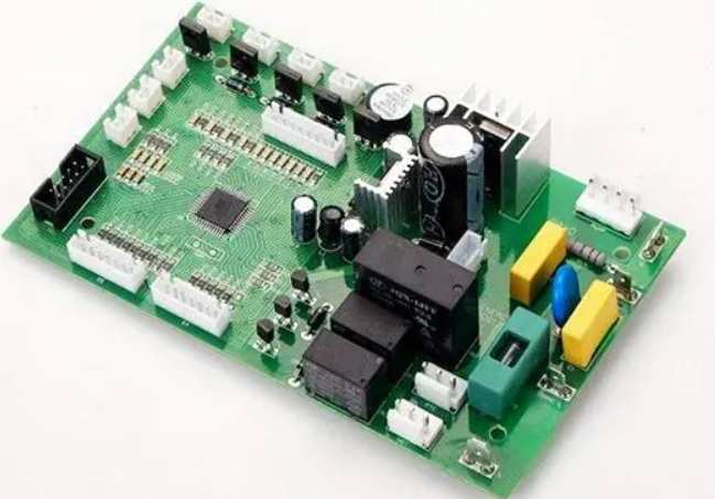
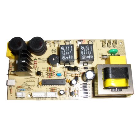
2. Inspection, testing and special process of PCBA
PCBA manufacturers need to go through a series of tests before the PCB SMT is processed and shipped, usually functional testing and online testing. These two types have complementary characteristics and are strictly tested according to customer quality requirements.
1. Functional test: Test the function of PCBA. If there is any display, the test tool verifies that the test command displays correct information on the screen.
2. Online testing: This kind of testing can check the defects of components in SMT processing.
I. Test method:
ICT: It is a way of testing all components simultaneously and can be done in a few seconds
Flying needle: The test lasts about 30 minutes. All components are tested with flying needles. The machine is programmed according to the layout of the circuit board to test each component
Two, special process:
1. After inspection and testing, the circuit board can be treated with special treatment, such as conformal coating, which is used to protect the PCBA in wet environment.
2. In the case of penetrating components, wave soldering and selective welding can be used to effectively improve the penetration rate of solder joints.
3. Causes and prevention methods of PCB circuit board distortion
The PCB circuit board distortion problem is often encountered in the processing and production of PCBA, which will have a great impact on the assembly and test of the subsequent process. Therefore, it is necessary to be familiar with the problem of PCB circuit board distortion, so as to avoid such phenomenon.
Causes of PCB circuit board distortion:
1, PCB circuit board itself caused by the material, single panel generally uses CIM-1, if the epoxide glass layer conversion temperature exceeds 110℃-130℃, the material is easy to distort.
2, PCB circuit board before heating, there is internal stress, it will cause the bending of the board, usually this stress is caused by improper design.
3. Improper fixture design. PCB circuit board equipment will age so that the glass of most laminates changes temperature, causing distortion after expansion.
Ways to prevent PCB circuit board distortion:
1, in the condition of not affecting the circuit board welding, as far as possible to lower the temperature.
2, circuit board design needs to be reasonable, each piece of copper foil area to balance.
3, in the case of price in line with expectations, recommend the use of international plate, choose high temperature resistant material, to prevent circuit board distortion.
The above is about the "PCB circuit board distortion causes and prevention methods" introduction, hope to have some help to you


Достаточно загрузить файлы Gerber, BOM и проектные документы, и команда KINGFORD предоставит полное предложение в течение 24 часов.