
Контрактное производство электроники под ключ в Китае
Шэньчжэнь, район Баоань, улица Фуюн, улица Фуцяо, район 3, промышленный парк Лонгхуй 6

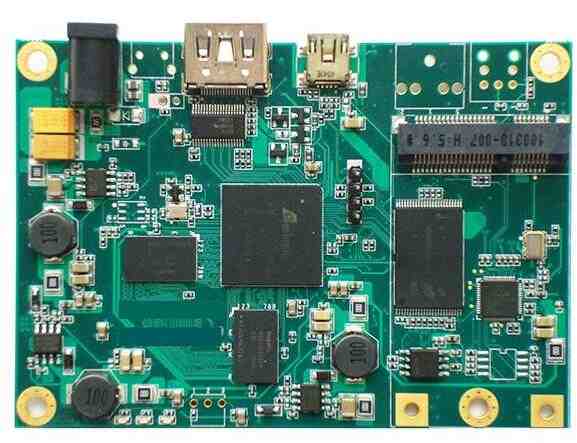
Today, various Emmc chip packages are being used in the direction of small and flat BGA, QFN, etc., and the price of adapters for such packages is not low. If there is an error in the production test and the production traceback is recalibrated, the chip must be removed from the adapter and re-run following the prescribed procedure, which is time consuming, laborious, and costly. The following patch manufacturer to say how to carry out IC programming in PCBA and how to carry out pcb circuit board design knowledge.
1. How to conduct IC programming in PCBA
The process of moving a program to the internal storage space of the chip is generally divided into offline burning and online burning offline burning. These chips are compatible with chips of different packages through various adapters, and the chips can be used with adapters to achieve program burning. The adapter itself is a precision fixture. Different chips and different packages require different adapters. Today, various Emmc chip packages are being used in the direction of small and flat BGA, QFN, etc., and the price of adapters for such packages is not low.
If there is an error in the production test and the production traceback is recalibrated, the chip must be removed from the adapter and re-run following the prescribed procedure, which is time consuming, laborious, and costly. Processing and producing PCbas can cause some surprises. If the temperature of the board is not high enough, the chip will deform when removed, which increases the risk of obsoletization. Online burning online programming uses the chip's standard communication bus, such as USB, SWD, JTAG, UART, etc. Interfaces are usually fixed and programmed with fewer pins attached. Since the interface communication rate is not high, the general cable can be used for combustion without high consumption. Because online burning is programmed through a wired connection, if an error is found during production testing, the faulty PCBA can be traced back and re-burned without removing the chip. It can not only save production cost, but also improve combustion efficiency.
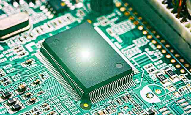
More importantly, the production line is moving towards automation. More and more manufacturers are adding functional test machines such as ICT and FCTS to the production line. The use of automatic fixtures and on-line combustion production methods can be omitted during the combustion phase. Manual operation, after the installation of the plate directly burned, and then send the PCBA to the test machine for testing, the whole production process is fully automated, can greatly improve the production efficiency. Therefore, the advantages of on-line combustion in PCBA processing are significant and have become one of the important indicators for measuring the process accuracy, production efficiency, cost, quality control, scale and capital of PCBA manufacturers. The IC is programmed using a debug/programming socket/probe prior to installation into the PCBA. Most PCBA institutions have programming interfaces for most Arm, AVR, and MSP430 MCUS.

2. How to design the pcb circuit board
An Electric Circuit Board (PCB) can be Printed by combining a large number of electronic components together, which saves a good amount of spare Space and does not interfere with the operation of the Circuit.
1. Enter the PCB design system and set relevant parameters
You can set the environment parameters of the design system according to your personal habits, such as the size and type of the grid and the size and type of the cursor. Generally speaking, you can use the default values of the system. In addition to the printed circuit board (Printed Circuit Board) size, the number of layers and other parameters are set
2. Generate the imported Network table
Network table is the bridge and link between Electric circuit schematic Design and Printed Circuit Board Design, which is very important. Network tables can be generated from circuit schematics or extracted from existing circuit board files. When network table is introduced, errors in circuit schematic design need to be inspected and corrected
3. Arrange the location of the packaging of each part
The automatic layout function of the system can be used, but the automatic layout function is not perfect, and the position of the package of each part needs to be adjusted manually
4, Electric circuit board wiring
The premise of automatic wiring of Electric circuit board is to set up safe distance, wire form and other contents. pcba assembly plant is an important electronic component, is the support body of electronic components, is the circuit connection provider of electronic components. Because it is produced by electronic printing technology, it is called "printed" circuit board. SMT manufacturers have high assembly density, small size and light weight of electronic products. The volume and weight of patch components are only about 1/10 of the traditional plug-in components. Generally, after SMT is adopted, the volume of electronic products is reduced by 40% ~ 60% and the weight is reduced by 60% ~ 80%. At present, the automatic wiring function of the equipment (shebei) is relatively perfect, and the general circuit diagram can be distributed through; However, the layout of some lines is not satisfactory and can also be done by hand
5. Output by printer or Save by hard copy
After wiring the circuit board, Save the completed circuit diagram file, and then use a variety of graphic output devices (shebei), such as printers or plotters to output the circuit board wiring diagram.
Comprehensive analysis of PCB RF technology
2023-02-12


Достаточно загрузить файлы Gerber, BOM и проектные документы, и команда KINGFORD предоставит полное предложение в течение 24 часов.