
Контрактное производство электроники под ключ в Китае
Шэньчжэнь, район Баоань, улица Фуюн, улица Фуцяо, район 3, промышленный парк Лонгхуй 6

There is a difference between a chip and a PCB
A PCB is a fiberglass board with copper traces that connect components. A chip is an electronic circuit made from a small flat piece of semiconductor material, usually silicon. The chip is placed in the housing. This is usually a small black box with pin connectors. Chips are generally smaller than PCBs, but more complex with specific functions. Chips may be placed on a single PCB as part of a multifunction device. Apple, for example, has more advanced chip manufacturing processes and is putting more features into its chips as they move away from Intel.

What are your thoughts on the subject of PCBs? PCB design can be quite complicated, but it's not too difficult if you're interested. Unless you're a designer or assembler, you probably won't believe the many myths surrounding these complex circuit boards. We've compiled a list of common misconceptions about PCB design to help you distinguish fact from fiction.
Myth 1 - All boards have the same design rules
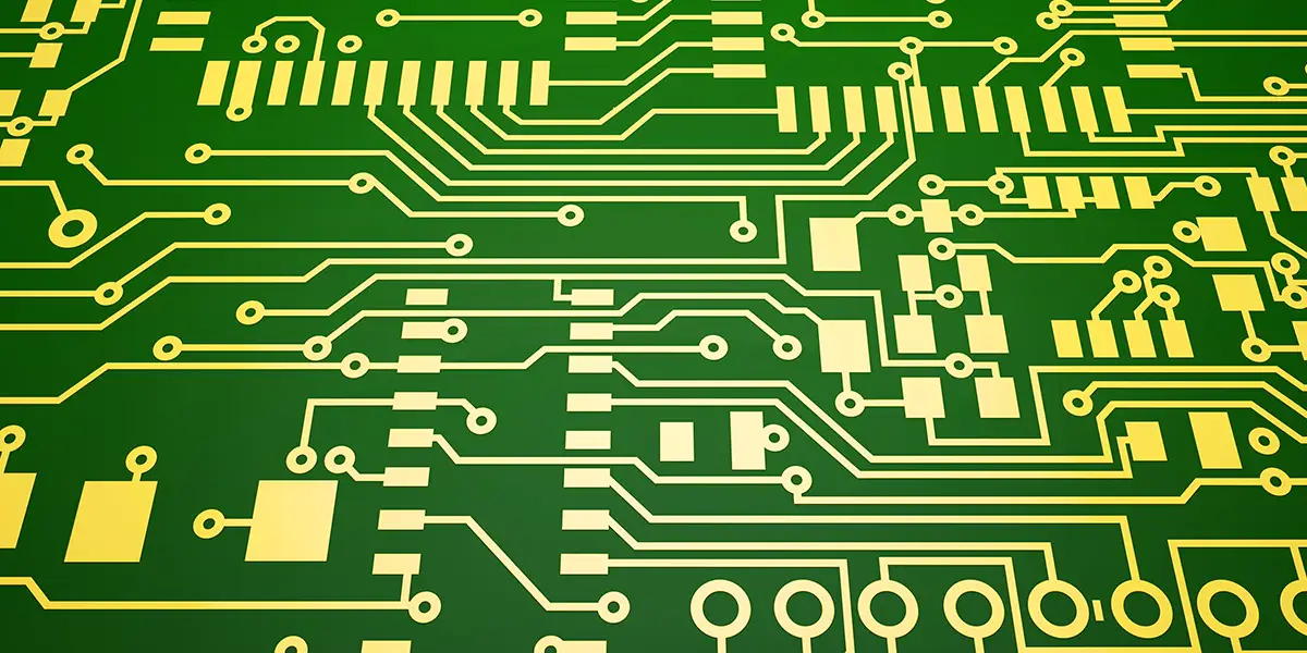
Printed Circuit Board Designs may vary. The composition and composition of PCBs are very similar. A typical circuit board will have two to four layers, each with a different thickness and copper weight. The base layers are the substrate, copper and solder mask. Screen printed PCBs are done for informational and functional purposes.
The main function of a circuit board is the basis of the manufacturing process and assembly. The design of the PCB is unique. You can think of it as a technical art form involving various works. All designs will not succeed if assembled according to the same rules and settings.
Myth 2: Component placement doesn't matter
Component placement is another common misconception about PCB design. While not all design rules apply to a specific PCB, careful consideration of component placement is critical to circuit performance. PCB designers cannot place components anywhere on the board or group similar parts together to save space. Designers must also consider heat and potential overload. Chips are becoming more sophisticated and more functional. This means less room for customization and repairs. Hope the chip is reliable and durable.
For clarity, consider the printed circuit board as a 3D model. Designers should consider both physical height and size when designing components. Each PCB assembly must be placed in a specific location for high-quality assembly. This is necessary to ensure that the electrical system does not overheat and reduce power consumption. Without this, today's technology will continue to fail.
Myth 3 - printed circuit boards are not environmentally friendly
While there is some truth to environmental concerns, there are ways to reduce your environmental impact. You may have heard that PCB manufacturing, design, assembly and manufacturing is not sustainable. The EPA states that the five processes of PCB manufacturing waste are: surface preparation, cleaning, catalyst application, electroless plating, pattern printing, masking and electroplating and etching. These include airborne particles and spent plating solution. Most electronic devices are not designed for permanent use, so reducing or recycling waste is critical. It is possible to be tech-savvy and still use products made by careless companies. Electronics sustainability is about manufacturing with non-toxic materials and recycling what companies can recycle.
Engineers will continue to work on biodegradable boards as a future target. Greener manufacturing processes are also possible.
From key fobs to electric blanket controllers, the ubiquitous and more popular PCB design remains an integral part of our tech industry. It doesn't matter if you're a designer or a user; it's a good idea to learn more about the subject before choosing a faster device from your computer.
Предыдущий: Нет


Достаточно загрузить файлы Gerber, BOM и проектные документы, и команда KINGFORD предоставит полное предложение в течение 24 часов.